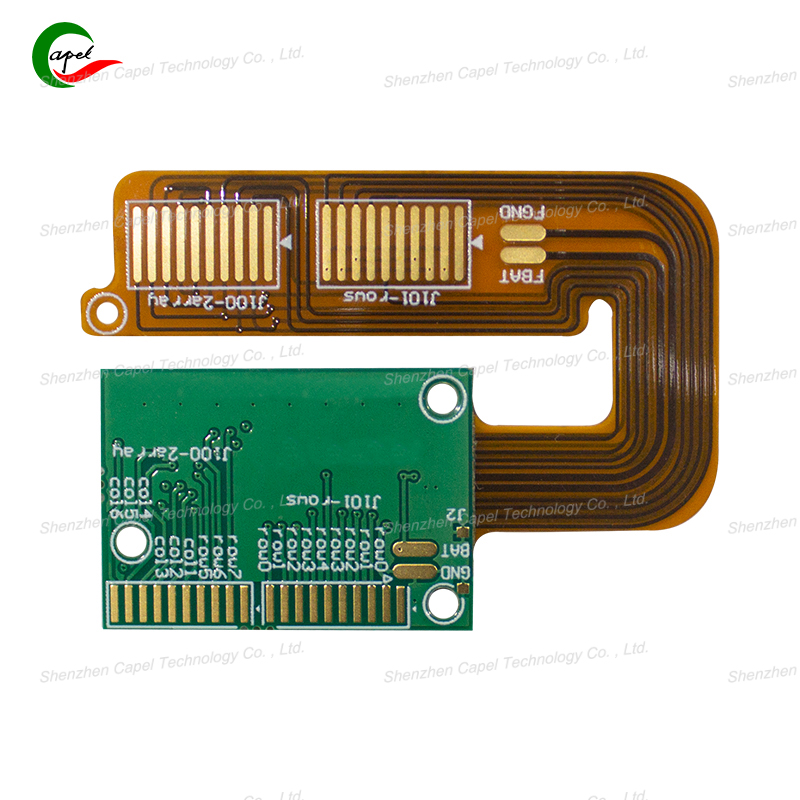
Rigid-flex PCBs mix stiff and bendable parts—so their production is a bit trickier than regular rigid or flexible PCBs. The two most critical steps are “bonding” (sticking rigid and flexible parts together) and “cutting” (shaping the board to fit devices). Let’s break down the whole process simply, with no confusing jargon—focusing on what matters for bonding and cutting.
It’s not rocket science—just a sequence of steps that blend rigid and flexible PCB manufacturing. Here’s how it works, step by step:
You need three key things:
-
Flexible substrate (usually polyimide, the bendable base).
-
Rigid substrate (FR-4, the stiff base used in regular PCBs).
-
Copper sheets (to make the circuits, same as other PCBs).
Factories cut these materials into the rough sizes they’ll need—no precise shapes yet.
This is like printing the “wires” on the boards:
-
Workers coat the copper sheets with a light-sensitive film, then shine a light through a stencil (with the circuit pattern).
-
The unexposed film is washed off, leaving the circuit pattern on the copper.
-
They etch away the extra copper—only the circuit lines stay.
This step is done for both the rigid FR-4 and flexible polyimide parts.
Now it’s time to attach the rigid and flexible sections. This is where precision matters—if they’re stuck wrong, the PCB won’t work. Here’s how factories do it:
-
They use a special adhesive (usually epoxy-based, super strong but thin).
-
The flexible part is aligned exactly with the rigid part (using machines that line up marks on both boards—like matching puzzle pieces).
-
They press the two parts together under heat (around 150-180°C) and pressure. The heat melts the adhesive, and when it cools, the parts are stuck tight—no gaps, no wiggling.
Just like regular PCBs, rigid-flex ones need holes to attach components (chips, sensors) or connect layers. Factories use tiny drills (some as thin as a hair) to make these holes—being careful not to crack the flexible parts.

The last big step is trimming the PCB to fit the device. Factories use two common methods, each with its own rules:
-
CNC routing: A small, precise machine with a rotating blade cuts the board. Good for complex shapes (like the curved edges of a smartwatch PCB).
-
Punching: For simple shapes (squares, rectangles), factories use a metal die to “punch” the shape out—fast and cheap.
Finally, they put a solder mask (the green/black layer you see) on the board to protect the circuits from moisture and dust. They also add a thin layer of gold or silver on the parts where components will be soldered.
Bonding isn’t just gluing two parts together—mess this up, and the PCB will break or fail. Here are the non-negotiable rules:
If the flexible part is off by even 0.1mm, the circuits won’t line up. Factories use cameras and computer-controlled machines to align the parts—no guesswork. A misaligned bond means the PCB can’t connect components properly.
Too thick, and the bond will be bulky—ruining the PCB’s ability to bend. Too thin, and it won’t stick. Most factories use adhesive that’s 0.05-0.1mm thick—thin enough to stay flexible, strong enough to hold for years.
Too much heat? The flexible polyimide will melt. Too little? The adhesive won’t set. Factories test the heat and pressure first with sample boards—making sure the bond is strong but the materials don’t get damaged.
Cutting might seem simple, but it’s easy to ruin the PCB if you’re not careful. Here’s what matters:
Factories map out the circuit lines first—so the cutting tool only trims the empty parts of the board. A wrong cut could slice through a copper line, killing the PCB.
Dull blades will “rip” the flexible polyimide instead of cutting it cleanly. Slow, sharp cuts leave smooth edges—so the PCB bends without cracking.
Cutting within 1mm of where the rigid and flexible parts are bonded can weaken the adhesive. Factories leave a small “buffer zone” around the bond—ensuring the cut doesn’t break the connection.
Making rigid-flex PCBs is about blending two different manufacturing processes—rigid and flexible. The bonding and cutting steps are where the “magic” (not real magic—just careful work) happens. Get those right, and you end up with a PCB that’s stiff where it needs to be, bendable where it should be.
related link: