Date: 2026-01-24
Have you ever wondered how the intricate green boards at the heart of all your electronics are actually made? Building a circuit board, or more accurately, manufacturing a Printed Circuit Board (PCB) and assembling it, is a fascinating journey from a digital idea to a physical, functional object. It’s less like “building” in a workshop and more like a precise, multi-stage industrial printing and assembly process.
Let’s walk through the key steps of how a circuit board comes to life, from a designer’s screen to a box of finished boards ready for your product.
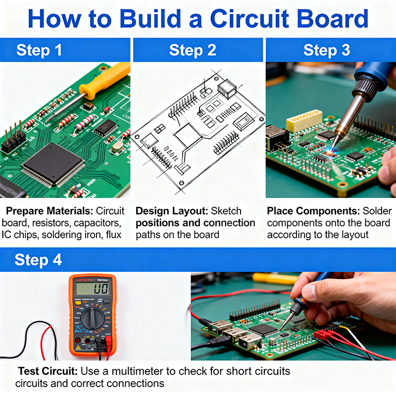
It all starts on a computer. Engineers use specialized software to design the circuit schematic and then lay out the physical board.
Schematic Capture: This is the “what connects to what” stage. Engineers place symbols for components (chips, resistors, connectors) and draw lines representing electrical connections.
PCB Layout: This is the “where everything goes” stage. The software helps arrange components on a virtual board and route the copper connection traces between them. Rules are set for trace width, spacing, and layer count. Think of it as an extremely complex, multi-layered city planning map for electricity.
Generating Manufacturing Files: Once the design is perfect, the software exports special files (most commonly Gerber files). These are like ultra-precise instructions for the PCB factory, detailing every copper layer, solder mask, and silkscreen layer. A Bill of Materials (BOM) listing every component is also prepared.

This is where the digital design gets turned into a physical board. A fabricator receives the Gerber files and begins a process that is part printing, part chemistry, and part precision machining.
Printing the Inner Layers: For multi-layer boards, the design for each inner copper layer is printed onto a photosensitive film, which is then used to transfer the pattern onto copper-clad laminate sheets.
Etching: The boards go through a chemical bath that etches away all the unwanted copper, leaving only the desired circuit traces behind. It’s like using acid to carve a intricate copper pathway.
Lamination and Drilling: All the inner and outer layers are stacked and fused together under heat and pressure into a single board. Then, a computer-guided drill creates all the necessary holes for through-hole components and vias (the tiny holes that connect layers).
Plating and Coating: The holes are plated with copper to make them conductive. Then, the entire board gets its iconic solder mask (usually green) applied to protect the copper, followed by the surface finish (like gold or silver) on the exposed pads to ensure they are solderable. Finally, any labels (the white silkscreen) are printed on.
The result is a bare PCB—a board with all the pathways, but no components attached.
Now, the empty board needs its electronic components. This is done through an automated, high-precision process.
Solder Paste Application: A stencil is placed over the board, and a machine spreads solder paste (a sticky mix of tiny solder balls and flux) onto all the component pads. It looks like using a screen-printing stencil.
Component Placement: A high-speed pick-and-place machine picks up components from reels or trays and places them with incredible accuracy onto their correct positions on the solder paste. This machine can place tens of thousands of parts per hour.
Reflow Soldering: The board travels on a conveyor through a reflow oven. This carefully heats the board in stages, melting the solder paste to form a permanent electrical and mechanical bond, then cooling it to solidify the joints.
Through-Hole and Final Assembly: Any remaining through-hole components are inserted, often by hand or with a specific machine, and the board may go through a wave soldering process. For complex boards, this might be followed by conformal coating for environmental protection.
Testing and Inspection: This is critical. Boards undergo Automated Optical Inspection (AOI) to check for placement defects, and electrical tests to ensure all connections are correct and the board functions as designed.
Building a circuit board at a professional level is a symphony of advanced design, material science, chemistry, and robotics. While it’s possible to make simple, single-layer boards at home with etching kits, the complex, multi-layer, high-density boards in modern devices are the product of sophisticated, automated factories.
Understanding this process helps demystify how your electronic products are made and highlights why choosing a manufacturing partner with tight control over each of these phases is so important for quality and reliability. It’s a remarkable journey from an idea to the technological foundation we hold in our hands every day.
Kaboer manufacturing PCBs since 2009. Professional technology and high-precision Printed Circuit Boards involved in Medical, IOT, UAV, Aviation, Automotive, Aerospace, Industrial Control, Artificial Intelligence, Consumer Electronics etc..