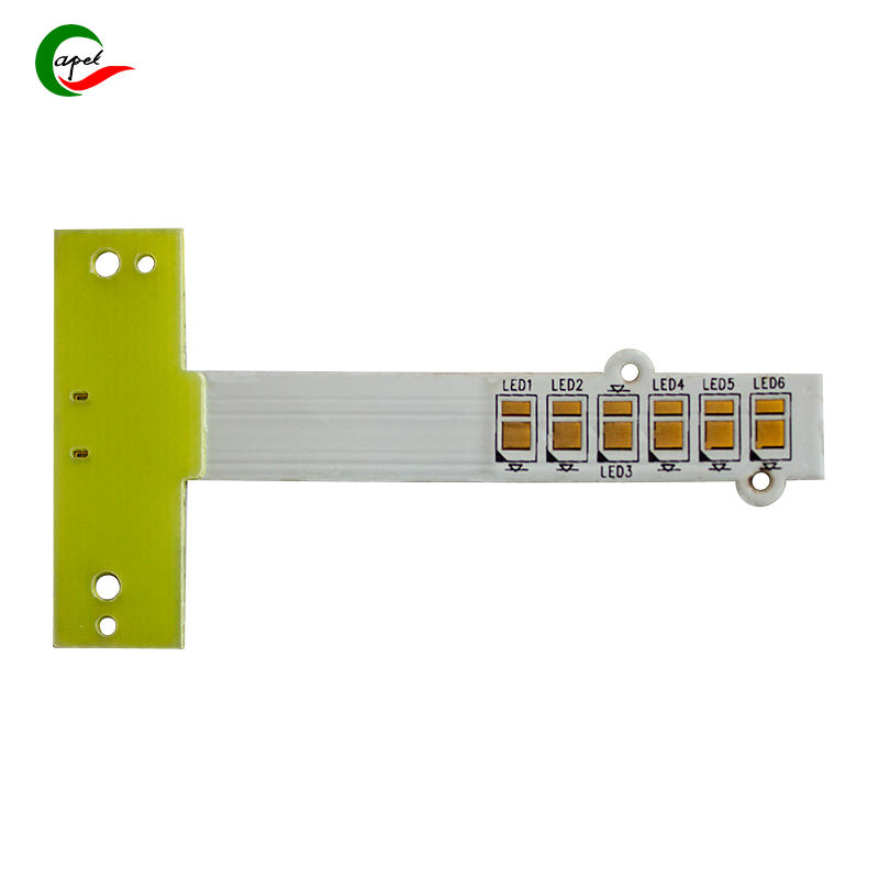
In the world of high-speed electronics—where 5G signals zip through smartphones, radar pulses enable autonomous driving, and medical devices transmit real-time data—impedance isn’t just a technical detail. It’s the invisible force that determines whether a flexible printed circuit (FPC) works flawlessly or fails catastrophically. For FPCs, which bend, twist, and fit into tight spaces, calculating impedance correctly is even more critical: a miscalculation can lead to signal loss, EMI interference, or complete system failure.
But how do you calculate impedance in a flexible circuit, where materials flex, layers shift, and designs are anything but rigid? This guide breaks down the science, the variables, and the tools that make accurate FPC impedance calculation possible.
Why Impedance Matters in FPCs
Impedance (measured in ohms, Ω) is the total opposition a circuit presents to the flow of alternating current (AC) signals. In high-speed applications (think 1+ Gbps data rates), even a small mismatch between the FPC’s impedance and the connected components (chips, connectors, antennas) causes signal reflection. This reflection corrupts data, creates delays, and generates electromagnetic interference (EMI) that can disrupt other parts of the system.
For FPCs, the stakes are higher:
- Their thin, flexible substrates (like polyimide) have different dielectric properties than rigid PCBs, altering impedance.
- Bending or flexing can slightly change the distance between conductors, shifting impedance over time.
- Compact designs (e.g., in wearables or foldables) force tight wire spacing, increasing the risk of crosstalk if impedance isn’t controlled.
In short: If your FPC’s impedance isn’t calculated and controlled—typically to 50Ω for most digital signals or 75Ω for video—your device won’t perform as designed.

Key Variables That Define FPC Impedance
Impedance in FPCs depends on a precise balance of physical and material properties. To calculate it, you first need to measure or define these critical variables:
1. Trace Geometry
The shape and size of the copper traces carrying the signal are foundational:
- Trace width (W): The width of the copper conductor (typically 0.05mm to 0.5mm in FPCs). Wider traces lower impedance; narrower traces raise it.
- Trace thickness (T): The height of the copper (often 9μm to 35μm). Thicker copper reduces resistance, slightly lowering impedance.
- Trace spacing (S): For differential pairs (two traces carrying complementary signals), the distance between them. Closer spacing increases coupling, reducing differential impedance.
2. Dielectric Properties
The insulating materials between traces and ground planes directly affect impedance:
- Dielectric constant (εr): A material’s ability to store electrical energy. Polyimide (PI), the most common FPC substrate, has an εr of 3.0–3.5. Higher εr lowers impedance (e.g., a substrate with εr=4.0 will reduce impedance compared to PI).
- Dielectric thickness (H): The distance between the signal trace and the nearest ground plane (or between two differential traces). Thicker dielectrics increase impedance; thinner ones decrease it.
3. Ground Plane Configuration
FPCs often use ground planes to stabilize signals and reduce EMI. The type of ground plane matters:
- Microstrip: A signal trace on top of the substrate, with a ground plane on the bottom. Common in single-sided FPCs.
- Stripline: A signal trace sandwiched between two ground planes. Used in double-sided or multi-layer FPCs for better shielding.
- Differential pairs: Two parallel traces with no dedicated ground plane (or a shared ground), designed to carry balanced signals (e.g., USB, Ethernet).
How to Calculate FPC Impedance: Methods and Tools
Calculating impedance manually is complex, but modern tools and formulas simplify the process. Here’s how engineers do it:
1. Empirical Formulas: For Quick Estimates
For simple FPC designs (e.g., microstrip or stripline), industry-standard formulas provide a starting point.
Microstrip Impedance (Z₀) Formula:
Used for single-sided FPCs with a signal trace on one side and a ground plane on the other:
Z₀ ≈ (87 / √(εr + 1.41)) × ln(5.98H / (0.8W + T))
Where:
- εr = dielectric constant of the substrate
- H = thickness of the substrate (distance from trace to ground)
Example: For a PI substrate (εr=3.2), H=0.1mm, W=0.2mm, T=0.018mm:
Z₀ ≈ (87 / √(3.2 + 1.41)) × ln(5.98×0.1 / (0.8×0.2 + 0.018)) ≈ 50Ω
Differential Pair Impedance (Z_diff) Formula:
For two parallel traces (common in high-speed FPCs):
Z_diff ≈ 2 × Z₀ × (1 – 0.48e^(-0.96S/H))
Where Z₀ is the single-ended impedance of one trace, and S is the spacing between the two traces.
2. Simulation Software: For Precision
Formulas work for simple designs, but FPCs with complex geometries (e.g., curved traces, varying dielectric layers, or reinforcement plates) require 3D electromagnetic simulation tools. These tools model the FPC’s physical structure and calculate impedance with high accuracy:
- Ansys HFSS: A gold-standard tool for 3D electromagnetic simulation. It accounts for FPC-specific variables like flex-induced trace deformation or material properties under temperature.
- Mentor HyperLynx: Popular for signal integrity analysis, it includes FPC-specific libraries for materials like PI and LCP (liquid crystal polymer).
- Altium Designer: Integrates impedance calculators into the PCB design workflow, ideal for engineers designing FPCs alongside rigid PCBs.
Simulators also account for real-world factors: How does bending the FPC affect trace spacing (and thus impedance)? Does a nearby reinforcement plate (like FR4) alter the dielectric environment? These nuances are critical for high-reliability applications like automotive radar or medical implants.
3. Prototyping and Testing: Validate Your Calculations
Even the best simulations need real-world validation. For FPCs, this means:
- Test coupons: Adding small, identical trace patterns (matching the FPC’s design) to the production panel. These coupons are measured with a time-domain reflectometer (TDR) to verify impedance.
- Environmental testing: Measuring impedance after temperature cycles (-40°C to 125°C) or flex cycles (10,000+ bends) to ensure it stays within tolerance (typically ±10% of the target value).
A leading FPC manufacturer for 5G devices, for example, uses TDR testing to confirm that their 50Ω differential pairs remain within 45–55Ω even after 100,000 bends—critical for foldable phone reliability.
Common Pitfalls to Avoid
Calculating FPC impedance isn’t just about plugging numbers into a formula. These mistakes can derail your results:
- Ignoring material variations: Not all PI substrates are identical—batch-to-batch variations in εr (±0.2) can shift impedance by 5Ω.
- Overlooking flex effects: Bending an FPC compresses the inner radius and stretches the outer radius, changing trace spacing and dielectric thickness. Simulate or test under flex conditions.
- Simplifying trace geometry: Curved or angled traces (common in FPCs) have different impedance than straight ones. Use 3D simulation for non-rectangular designs.
Conclusion: Impedance Calculation = Reliability
In high-speed FPCs, impedance calculation isn’t an afterthought—it’s the foundation of performance. Whether you’re using formulas for quick estimates, 3D simulators for precision, or TDR testing for validation, the goal is the same: ensure signals flow without reflection, interference, or loss.
For engineers designing the next generation of flexible electronics—from foldable displays to IoT sensors—mastering FPC impedance calculation isn’t just a skill. It’s the key to turning innovative designs into reliable, market-ready products.
After all, in a world where every microsecond and every decibel matters, impedance is the invisible metric that makes or breaks success.
Founded in 2009, our company has deep roots in the production of various circuit boards. We are dedicated to laying a solid electronic foundation and providing key support for the development of diverse industries.
Whether you are engaged in electronic manufacturing, smart device R&D, or any other field with circuit board needs, feel free to reach out to us via email at sales06@kbefpc.com. We look forward to addressing your inquiries, customizing solutions, and sincerely invite partners from all sectors to consult and collaborate, exploring new possibilities in the industry together.
