Flexible printed circuits (FPCs) are the unsung heroes of modern electronics, enabling devices to bend, twist, and fit into spaces rigid PCBs can’t. But designing an FPC that’s reliable, cost-effective, and fit for its purpose requires more than just swapping a rigid substrate for a flexible one. It demands a nuanced understanding of how flexibility impacts performance, durability, and manufacturability. Whether you’re designing for a foldable phone, a medical sensor, or an automotive hinge, these key design principles will ensure your FPC meets its goals—without costly rework or field failures.
1. Material Selection: The Foundation of Flexibility
The materials you choose dictate an FPC’s flexibility, temperature resistance, and signal performance. Balancing these factors is critical for engineers working on cutting-edge devices:
- Substrates: Polyimide (PI) is the gold standard for most FPCs, offering excellent heat resistance (-269°C to 400°C) and flex life. For high-frequency applications (like 5G wearables), liquid crystal polymer (LCP) substrates minimize signal loss at 60GHz+. For cost-sensitive devices (e.g., basic fitness trackers), polyester (PET) works but sacrifices high-temperature durability.
- Copper: Rolled annealed (RA) copper is essential for FPCs that bend repeatedly (e.g., foldable phone hinges). Its ductile structure withstands 100,000+ flex cycles without cracking, unlike brittle electrodeposited (ED) copper, which is better suited for static FPCs (e.g., camera connectors).
- Adhesives: Adhesiveless laminates (bonding copper directly to PI) reduce thickness and improve flex life, making them ideal for ultra-thin wearables. For high-reliability applications (aerospace), epoxy adhesives with high glass transition temperatures (Tg ≥ 150°C) prevent delamination under thermal stress.
2. Trace Routing: Balancing Signal Integrity and Flexibility
FPC traces carry power and data, but their design must account for both electrical performance and mechanical stress:
- Trace width and spacing: Wider traces (0.2mm+) handle higher currents (critical for battery-powered wearables) but reduce flexibility. For high-speed signals (e.g., USB 3.2), maintain controlled impedance (50Ω ±5%) with precise width (0.1mm–0.15mm) and spacing from ground planes. Use simulation tools like Altium Designer to validate impedance before prototyping.
- Avoid sharp angles: 90° corners concentrate stress during bending, leading to trace cracks. Replace them with 45° angles or rounded corners (radius ≥ 0.5mm) to distribute stress evenly—essential for FPCs in smartwatch hinges or robotic arms.
- Ground planes: Include a continuous ground plane (connected to chassis ground) to shield sensitive signals from EMI. In multi-layer FPCs, sandwich signal layers between ground planes to minimize crosstalk, a must for medical devices with ECG sensors.
3. Bend Area Design: The Make-or-Break Zone
The bend area is where most FPC failures occur. Designing it to withstand repeated flexing requires careful attention to geometry and material distribution:
- Bend radius: Follow the "10x rule": The minimum bend radius should be 10x the FPC’s total thickness. For a 0.1mm thick FPC, that means a radius of at least 1mm. Tighter radii (common in foldable phones) demand thinner substrates (12μm PI) and RA copper to avoid cracking.
- Avoid components in bend zones: Surface-mount devices (SMDs) in areas that flex will suffer solder joint failures. Relocate components to rigid sections or use reinforcement plates (FR4 or stainless steel) to stabilize them—critical for automotive FPCs in door hinges.
- Uniform layer thickness: Ensure the FPC’s cross-section is symmetric around the bend axis. Uneven layers (e.g., a thick adhesive on one side) cause warping during flexing, a problem in AR glasses where precise alignment is key.
4. Reinforcement: Strategic Stiffness Where Needed
FPCs need rigidity in specific areas (e.g., connector tabs) without sacrificing flexibility elsewhere. Smart reinforcement design prevents costly failures:
- Material matching: Use FR4 reinforcement for connector tabs in consumer electronics (e.g., charging ports) for its cost-effectiveness and rigidity. For high-vibration environments (automotive engine bays), stainless steel reinforcement adds strength and EMI shielding.
- Size and placement: Reinforcements should extend 1–2mm beyond the area needing support (e.g., a connector’s solder pads) to distribute stress. In medical patches, polyimide reinforcement around sensor contacts ensures reliable skin contact without restricting flex.
- Adhesive selection: Use heat-cured epoxy adhesives (instead of pressure-sensitive adhesives) for reinforcement bonding—they withstand temperature cycles better, a must for EV battery FPCs.

5. Manufacturing Considerations: Design for Manufacturability (DFM)
Even the best FPC design fails if it’s hard to produce. Prioritizing DFM reduces costs and lead times:
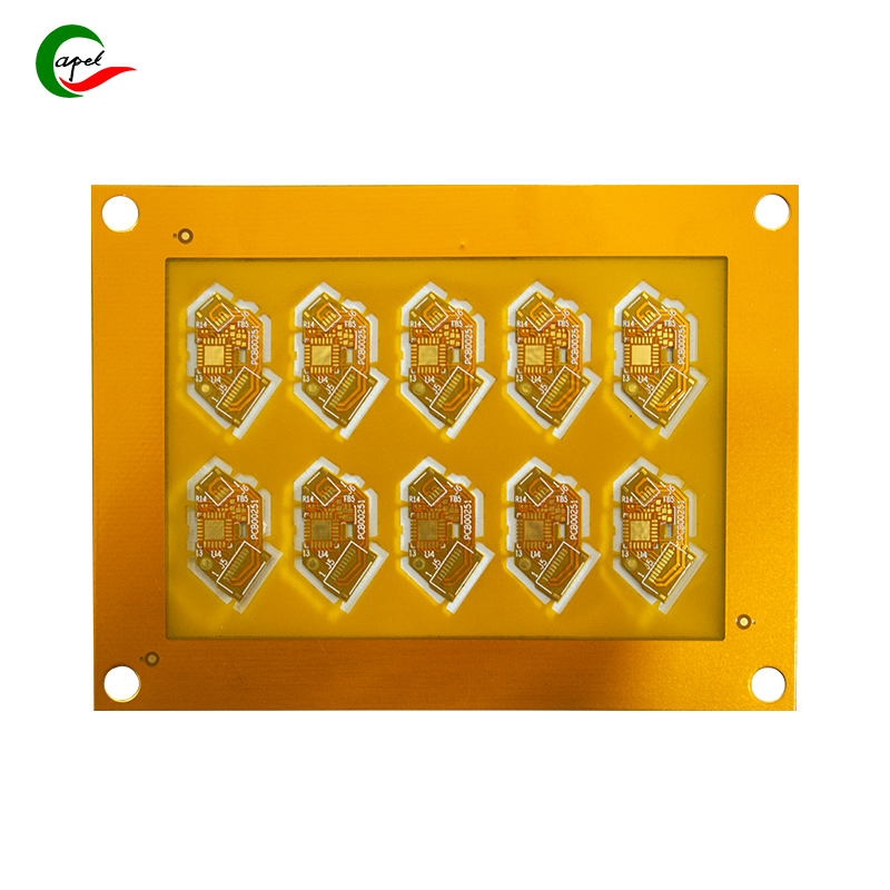
- Panelization: Arrange FPCs on production panels with 2–3mm spacing to avoid damage during routing. For high-volume runs (e.g., smartphone flex cables), use roll-to-roll processing with 50mm+ web widths for efficiency.
- Tooling holes: Include 1–2mm diameter tooling holes in non-critical areas to align the FPC during lamination and etching. This reduces misalignment defects, which are costly to fix in multi-layer FPCs.
- Clearances: Maintain at least 0.1mm clearance between traces and the FPC edge to prevent copper exposure during cutting. For flex-to-rigid transitions, ensure 0.5mm clearance between the rigid reinforcement and flexible area to avoid delamination.
6. Testing and Validation: Proving Reliability
FPCs face unique stresses, so testing must go beyond standard PCB checks:
- Flex cycle testing: Subject prototypes to 100,000+ bend cycles (180° at the designed radius) and monitor for resistance changes (should be <5%). This is non-negotiable for foldable devices or wearable bands.
- Thermal cycling: Test from -40°C to 85°C (or higher for automotive) to check for delamination or solder joint cracks. Use X-ray inspection to detect hidden defects in multi-layer FPCs.
- Impedance testing: Verify controlled impedance with a time-domain reflectometer (TDR) to ensure signal integrity in high-speed applications (e.g., 5G antennas).
Case Study: Designing FPCs for Foldable Phones
Leading foldable device models illustrate best practices in FPC design:
- Bend zone optimization: The hinge FPC uses 12μm PI substrate and 18μm RA copper with a 1.5mm bend radius, surviving 200,000+ folds.
- Reinforcement strategy: FR4 reinforcement at the display connector prevents tab warping, while the rest of the FPC remains flexible.
- Signal integrity: LCP-based traces with 50Ω impedance ensure 4G/5G signals pass through the hinge without loss.
Conclusion: FPC Design = Balance
Designing an FPC is a dance between flexibility and rigidity, performance and manufacturability. By selecting the right materials, optimizing trace routing, engineering bend zones carefully, and designing for production, you’ll create FPCs that enable innovation—whether in a life-saving medical device or the next breakthrough in consumer tech.
Mastering these design points isn’t just about avoiding failures. It’s about staying competitive in a market where flexibility isn’t a luxury—it’s a requirement.
Founded in 2009, our company has deep roots in the production of various circuit boards. We are dedicated to laying a solid electronic foundation and providing key support for the development of diverse industries.
Whether you are engaged in electronic manufacturing, smart device R&D, or any other field with circuit board needs, feel free to reach out to us via email at sales06@kbefpc.com. We look forward to addressing your inquiries, customizing solutions, and sincerely invite partners from all sectors to consult and collaborate, exploring new possibilities in the industry together.
