
Date: 2026-07-16
You're designing a new electronic product. Maybe an industrial controller, a communication device, an automotive module, or an AI compute board. Your schematic keeps growing, components are multiplying, signal speeds are climbing. You've pushed your double-sided board to its absolute limit — signal integrity is a nightmare, and the product crashes randomly.
You need a multilayer PCB.
A multilayer PCB is a board with three or more conductive copper layers. Compared to single-sided and double-sided boards, multilayer boards separate power planes, ground planes, and signal layers — giving you cleaner signals, more routing space, and smaller products. In this guide, I'll walk you through the fundamentals of multilayer PCB design — from stackup to design rules — in plain English.
A stackup is simply the arrangement of copper and insulating layers from top to bottom. It's not random — the stackup determines signal integrity, impedance control, and EMI performance. Once the layers are laminated, you're stuck with them.
In multilayer boards, the stackup determines several critical electrical properties — signal integrity, impedance control, and electromagnetic compatibility. High-speed digital signals behave more like electromagnetic waves than simple currents, so the physical structure of the PCB plays a major role in how they propagate.
Rule 1: Every Signal Layer Needs an Adjacent Reference Plane
This is the single most important stackup rule. Every signal layer should reference at least one continuous adjacent plane (ground or power), with no unrelated routing layer in between.
Why? At high frequency, return current concentrates directly under the signal trace on the nearest reference plane. If there's no adjacent plane, the return current travels farther to find a reference — larger loop area = more inductance, more ringing, more radiated emissions.
Rule 2: The Stackup Must Be Symmetrical
Mechanical stability is just as important as electrical performance. Warpage happens when thermal expansion forces are unbalanced — usually caused by an asymmetric stackup where copper weight isn't mirrored around the center axis. During reflow at 230-250°C, materials expand at different rates — an asymmetric stackup causes the board to bend, leading to head-in-pillow issues on BGA packages.
Rule 3: Keep Power and Ground Planes Tightly Coupled
The closer the power and ground planes, the larger the distributed capacitance between them. This inherent capacitance reduces high-frequency noise without extra decoupling devices. A 4-mil dielectric spacing between tightly-paired power and ground planes yields about 90 pF per square inch.
Rule 4: Route High-Speed Signals as Stripline, Not Microstrip
Microstrip is a trace on an outer layer with a reference plane on one side and air on the other. Part of its field is in the air — more susceptible to radiation and external coupling.
Stripline is a trace with solid reference planes on both sides. It contains the electric field completely between the two planes. For high-speed signals where EMI containment is critical, stripline is strongly preferred. The catch? Stripline needs at least 6 layers.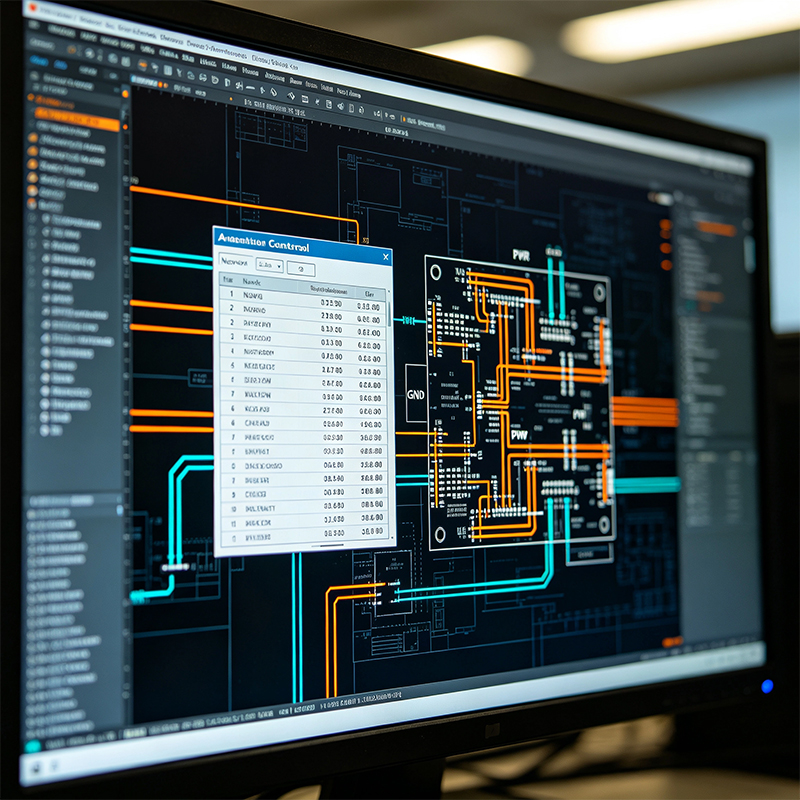
4-layer: Signal-Ground-Power-Signal. High-speed signals on the outer layers, inner layers for reference planes. The entry-level multilayer, great for most moderate-speed applications.
6-layer: Signal-Ground-Signal-Power-Ground-Signal. More signal layers, more routing flexibility. Inner signals can be stripline, better signal quality.
More layers = better routing and signal quality, but higher cost. High-end designs can go to 20+ layers.
High-speed signals need controlled impedance. USB 3.0 requires 90Ω differential impedance, PCIe requires 85Ω, and DDR4 data lines must be precisely matched. Impedance depends on trace width, copper thickness, distance to the reference plane, and dielectric constant.
Target tolerance is ±10%. Don't use generic formulas — different manufacturers use different materials, and variations can exceed 10%.
FR4: The workhorse — great value. Works for applications below 3GHz.
High-frequency materials (Megtron 6, Rogers): Minimal signal loss — for 5G and radar.
Hybrid stackups: Rogers for high-speed layers, FR4 for power/ground. Can save 40-60% in material cost.
Good design must be manufacturable:
Aspect ratio: Board thickness divided by hole diameter — keep it reasonable
Annular ring: Enough copper around each drilled hole
Copper symmetry: Prevent warpage
IPC-2221: Foundation design standard — covers trace width, spacing, vias, stackup
IPC-2222: Rigid PCB design
IPC-2315 / IPC-2226: HDI design standards
In multilayer PCB design, the stackup is the single most important decision you'll make. Every signal layer needs an adjacent reference plane. The stackup must be symmetrical. Route high-speed signals as stripline, not microstrip. Control impedance to ±10%.

Kaboer manufacturing PCBs since 2009. Professional technology and high-precision Printed Circuit Boards involved in Medical, IOT, UAV, Aviation, Automotive, Aerospace, Industrial Control, Artificial Intelligence, Consumer Electronics etc..


 English



 Wechat
 +86 13670210335
 +86 13670210335
 E-mail