Date: 2025-12-16
In the race to make gadgets smaller, smarter, and more integrated, one component quietly powers the revolution: the small circuit board. More than just a scaled-down version of its larger counterpart, these miniaturized marvels represent the frontier of electronic design and manufacturing, packing immense functionality into a tiny footprint.
For product designers and OEMs worldwide, mastering small circuit boards is no longer a niche skill—it's a core requirement for innovation. Let's explore what defines them, why they're critical, and the unique expertise required to build them reliably.
A small circuit board, often called a mini PCB or compact PCB, is typically characterized by its dimensions and design philosophy. While there's no universal standard, boards with a diagonal under 100mm (about 4 inches) or those designed to fit within exceptionally tight enclosures (like wearables or medical implants) fall into this category.
However, size is only half the story. What truly defines a modern small circuit board is its high-density design. This means it achieves maximum functionality per square centimeter through:
High-Density Interconnect (HDI): Utilizing micro-vias, blind vias, and buried vias to create more connections in less space.
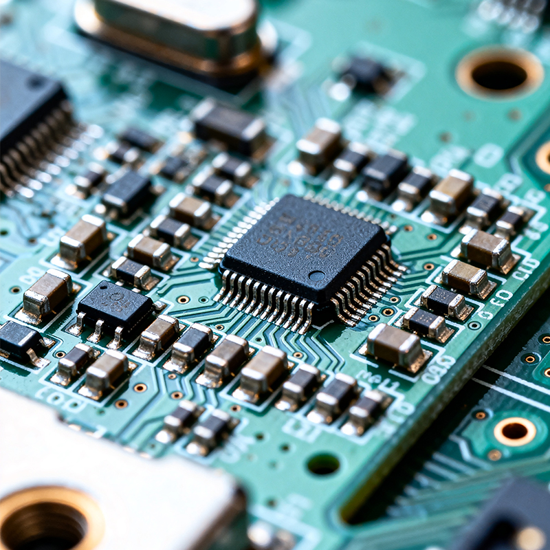
Fine-Pitch Components: Populating the board with tiny packages like 01005 resistors/capacitors, chip-scale packages (CSP), and micro BGAs.
Multi-Layer Design: Stacking 4, 6, 8, or more layers in a thin profile to route complex circuitry.
They are the foundational hardware for the Internet of Things (IoT), wearable technology, advanced medical devices, and miniaturized consumer electronics.
Why is there such a relentless drive toward miniaturization? The benefits are transformative for end products:
1. Enabling Product Innovation
Small circuit boards are the key enabler for entire product categories. Without them, there would be no smartwatches that track your health, no wireless earbuds with active noise cancellation, and no pill-sized endoscopic cameras. They allow designers to reimagine form factors and create devices that integrate seamlessly into our lives and environments.
2. Enhancing Portability and Wearability
This is the most obvious advantage. Reducing the size and weight of the core electronics directly translates to lighter, more comfortable, and truly portable devices, from handheld scanners to fitness trackers.
3. Improving Performance and Efficiency
Miniaturization often goes hand-in-hand with optimization. A tightly integrated small board can have shorter signal paths, which reduces interference, improves signal integrity for high-speed data, and can lower power consumption—a critical factor for battery-powered devices.
4. Reducing Overall System Cost
While the individual small board might be complex, it can often consolidate functions that previously required multiple larger boards and connectors. This simplifies overall assembly, can reduce material usage, and lowers the total bill of materials for the final product.
Designing a small circuit board is one thing; manufacturing it consistently and reliably is another. This is where expertise separates concept from quality production.
Precision is Paramount: Solder paste deposition, component placement, and etching tolerances are measured in microns. A shift of a few thousandths of a millimeter can cause bridging or open connections.
Material Selection: Thin, high-performance laminates are often required to maintain reliability in a slim, multi-layer stack-up. The choice of solder mask and surface finish also becomes more critical.
Advanced Assembly Processes: Standard SMT lines may need specialized nozzles and high-precision vision systems to handle micro-components. Techniques like Underfill for CSPs or Precision Glue Dispensing may be necessary for reliability.
Rigorous Testing: In-circuit test (ICT) probes may be too large for densely packed boards. Flying probe testing, enhanced automated optical inspection (AOI), and functional testing become essential to guarantee yield.
At Kaboer, based in the heart of Shenzhen's electronics ecosystem, we understand that small circuit boards demand outsized attention to detail. Our manufacturing focus is tailored to meet these precise demands.
Our in-house factory is equipped with the necessary technology—from high-precision stencil printers and chip shooters capable of handling 01005 components to advanced inspection systems—to navigate the challenges of miniaturization. We combine this with a stringent quality management process to ensure that every small board we ship is not just functionally complete, but robust and reliable.
For innovators looking to turn a compact, powerful concept into a tangible, high-quality product, partnering with a manufacturer experienced in the nuances of small circuit boards is a crucial step.
Kaboer manufacturing PCBs since 2009. Professional technology and high-precision Printed Circuit Boards involved in Medical, IOT, UAV, Aviation, Automotive, Aerospace, Industrial Control, Artificial Intelligence, Consumer Electronics etc..