Date: 2026-01-22
Let’s talk about how the circuit boards inside your products actually come to life. When you imagine a factory making electronics, you might picture rows of people with soldering irons, meticulously placing tiny parts. That image is about 40 years out of date.
Today, the process is called SMT PCB Assembly (Surface Mount Technology Printed Circuit Board Assembly), and it looks more like a highly choreographed dance of robots, ovens, and laser-sharp cameras. It's fast, precise, and the reason you can hold a supercomputer in your pocket.
If you're sourcing electronics, understanding this process isn't just technical trivia—it's the key to evaluating manufacturers, anticipating challenges, and ensuring you get quality boards on time.
First, a quick why. Before SMT, we used "through-hole" assembly, where parts had long legs that went through holes in the board. It was sturdy but slow, manual, and limited how small things could get.
SMT flips the script. Components (now called SMDs - Surface Mount Devices) are flat, with little metal pads instead of legs. They sit on the surface of the board. This one change made everything smaller, faster, and cheaper at scale. Your smartphone, your smartwatch, your Wi-Fi router—they all exist because of SMT.
So, how does a blank PCB become a populated, functioning assembly? Let's walk the line.
This is where the "glue" is applied. A stainless steel stencil, laser-cut with holes matching the board's solder pads, is aligned over the PCB. A squeegee pushes solder paste—a sticky mix of microscopic solder balls and flux—across the stencil, depositing a precise amount onto every pad.
Think of it like: Using a stencil to spray-paint a perfect design. The accuracy here is everything. Too little paste, and the joint will be weak. Too much, and you risk short circuits.
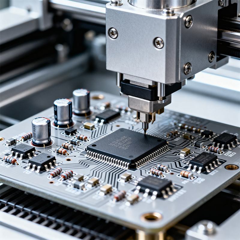
This is the star of the show. A pick-and-place machine takes over. It has reels and trays of all your components. Using a tiny vacuum nozzle, it picks up resistors, chips, capacitors—some smaller than a grain of sand—and places them onto the wet solder paste pads at incredible speeds (tens of thousands of parts per hour).
The nuance isn't just speed: It's about precision, vision systems to correct for tiny board variations, and handling components so delicate that a puff of air can blow them away.
Now, we make the connections permanent. The board travels on a conveyor through a reflow oven. This isn't a simple heater; it's a carefully tuned thermal tunnel with distinct zones:
Preheat: Gently brings the board up to temperature.
Soak: Activates the flux in the paste and equalizes heat.
Reflow: A brief spike above the solder's melting point (around 240°C/464°F), causing it to flow and form a metallurgical bond.
Cooling: A controlled solidification to create strong, shiny solder joints.
This step is pure chemistry and physics. The wrong temperature profile can lead to tombstoning (where a component stands up on one end), cold joints, or damaged parts.
You can't ship 10,000 boards and hope they work. This is where quality is enforced.
Automated Optical Inspection (AOI): Cameras scan the board from multiple angles, comparing it to the perfect digital design. It catches missing, misaligned, or poorly soldered components.
X-Ray Inspection: For components like BGAs where the solder joints are hidden underneath the chip, X-ray machines see right through to verify a perfect connection.
Functional Testing: Finally, the board might be powered up in a test fixture to verify it performs as intended.
A factory with the latest equipment can still produce garbage. The real differentiator is the team around the machines.
Process Engineers: They're the ones constantly monitoring solder paste viscosity, tweaking oven profiles, and optimizing machine programs. They turn equipment into a reliable process.
Component Librarians: Every single component needs a perfect digital footprint in the machine's system—its size, pick-up point, and orientation. A mistake here means misplacement.
Quality Control Technicians: They interpret AOI and X-ray results, perform manual checks, and own the final "go/no-go" decision.
When you're evaluating a manufacturer for your SMT PCB assembly, here are the practical questions to ask:
How do you handle component sourcing and shortages? (A factory in Shenzhen, like Kaboer, has a massive advantage here due to local supply chains.)
What's your first-pass yield? (What percentage of boards pass all tests right off the line? This tells you about process control.)
Can I see your DFM (Design for Manufacturability) report? A good partner will review your design files before production and suggest changes to improve yield and reliability.
What happens if there's an issue? Is there a direct line to the production floor for problem-solving?
SMT PCB assembly is the bedrock of modern electronics manufacturing. It’s a sophisticated, interconnected process where material science, precision mechanics, and strict process control converge.
For you, the manufacturer, success means finding a partner who treats this process with the seriousness it deserves—a partner that sees itself not just as a "board stuffer," but as an extension of your engineering team. You want the confidence that comes from knowing your designs are being built with expertise, care, and a relentless focus on getting it right the first time.
Kaboer manufacturing PCBs since 2009. Professional technology and high-precision Printed Circuit Boards involved in Medical, IOT, UAV, Aviation, Automotive, Aerospace, Industrial Control, Artificial Intelligence, Consumer Electronics etc..