Date: 2025-12-18
Open up any modern gadget—a smartphone, a smartwatch, your car's infotainment system. You'll see a green board covered in tiny, flat silver components. What you're looking at is the result of SMT soldering, the dominant manufacturing process that makes modern electronics possible. It's the precise, high-volume method for attaching surface-mount components to a PCB, forming millions of reliable electrical connections that are often invisible to the naked eye.
For any electronics manufacturer, the quality of SMT soldering isn't just a step in production; it's the single most critical factor determining your product's reliability, performance, and longevity. Getting it wrong means field failures, recalls, and damaged reputations. Let's break down what this process truly entails.
SMT Soldering (Surface Mount Technology Soldering) is the automated process of forming permanent electrical and mechanical bonds between surface-mount components and a printed circuit board using solder. Unlike old-school through-hole soldering (where leads go through holes), SMT components sit directly on the board's surface.
The goal is deceptively simple: melt a precisely controlled amount of metal alloy (solder) to create a perfect "fillet" connecting the component's metal termination to the PCB's copper pad. But achieving millions of these perfect connections consistently is an engineering feat.
The core of SMT soldering is the reflow soldering process. Think of it as a carefully choreographed thermal dance with four key acts:
Solder Paste Application (The Blueprint): First, a stainless-steel stencil is aligned over the PCB. A squeegee forces solder paste—a sticky mixture of microscopic solder balls and flux—through the stencil's openings onto the exact pads where components will sit. This deposit's volume and shape are critical.
Component Placement (The Precision Pick-and-Place): Robotic machines, guided by high-resolution cameras, pick components from reels or trays and place them with astonishing accuracy (within ±25 microns) onto the solder paste deposits. The paste's tackiness holds them temporarily in place.
Reflow Soldering (The Thermal Transformation): This is the heart of the process. The populated board travels on a conveyor through a multi-zone reflow oven. It goes through a precise thermal profile:
Preheat: Gradually raises the temperature to activate the flux and prevent thermal shock.
Soak/Thermal Equalization: Allows the entire board and all components to reach a uniform temperature.
Reflow (Peak): The temperature quickly rises past the solder's melting point (typically 217-250°C for lead-free). The solder balls melt, coalesce, and, driven by surface tension and flux action, wick up to form a smooth, shiny joint between the pad and component.
Cooling: Controlled cooling solidifies the joints, completing the bond.
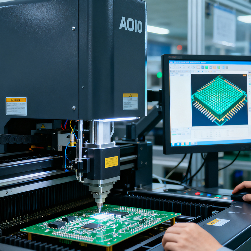
Cleaning & Inspection (The Quality Gate): For certain pastes, boards may be cleaned. Then, Automated Optical Inspection (AOI) systems use cameras to scan every joint for defects like insufficient solder, bridging, or misalignment.

This process is the backbone of electronics for compelling reasons:
Enables Miniaturization: SMT components can be incredibly small (like 01005 packages, just 0.4mm x 0.2mm). The process allows for ultra-high-density designs impossible with through-hole parts.
Superior Speed & Consistency: It's fully automated, allowing thousands of perfect joints to be formed simultaneously and consistently across every board—vital for high-volume production.
Enhanced Performance: Shorter electrical paths and smaller parasitic inductance/capacitance in SMT joints enable better high-frequency and high-speed circuit performance.
Cost-Effectiveness: Higher automation, fewer drilled holes, and compatibility with double-sided assembly reduce overall manufacturing costs.
Not all SMT soldering is equal. Success depends on mastering variables:
Paste Quality & Printing: Poor paste or a misaligned stencil leads to skipped or uneven deposits.
Thermal Profile: An incorrect profile can cause cold solder joints (weak, grainy connections), tombstoning (components standing up), or thermal damage to sensitive parts.
Pad Design: PCB pads must be correctly sized and spaced for the component to allow proper solder fillet formation.
A perfect SMT solder joint under a microscope looks like a smooth, concave "fillet" with a shiny surface—the visual hallmark of a strong, reliable metallurgical bond.
From consumer tech to life-saving devices, this process is universal:
Consumer Electronics: The foundation of all smartphones, tablets, and laptops.
Automotive: Engine control units, sensors, and infotainment systems.
Medical: Critical for miniaturized, reliable devices like pacemakers and monitoring equipment.
Industrial: Rugged controllers, robotics, and power management systems.
At Kaboer, based in the manufacturing hub of Shenzhen, we know that SMT soldering is where theory meets reality. Our factory is built around controlling this critical process. We invest in high-precision stencil printers, maintain rigorously calibrated reflow ovens with detailed thermal profiling for every board type, and utilize advanced AOI and X-ray systems to verify what the human eye cannot see. This disciplined focus on the fundamentals of SMT soldering is what ensures the boards we build don't just function on the test bench, but endure in the real world.
For a partner that treats every solder joint as a commitment to your product's success, look to a manufacturer who masters the art and science of SMT.
Kaboer manufacturing PCBs since 2009. Professional technology and high-precision Printed Circuit Boards involved in Medical, IOT, UAV, Aviation, Automotive, Aerospace, Industrial Control, Artificial Intelligence, Consumer Electronics etc..