Date: 2026-02-03
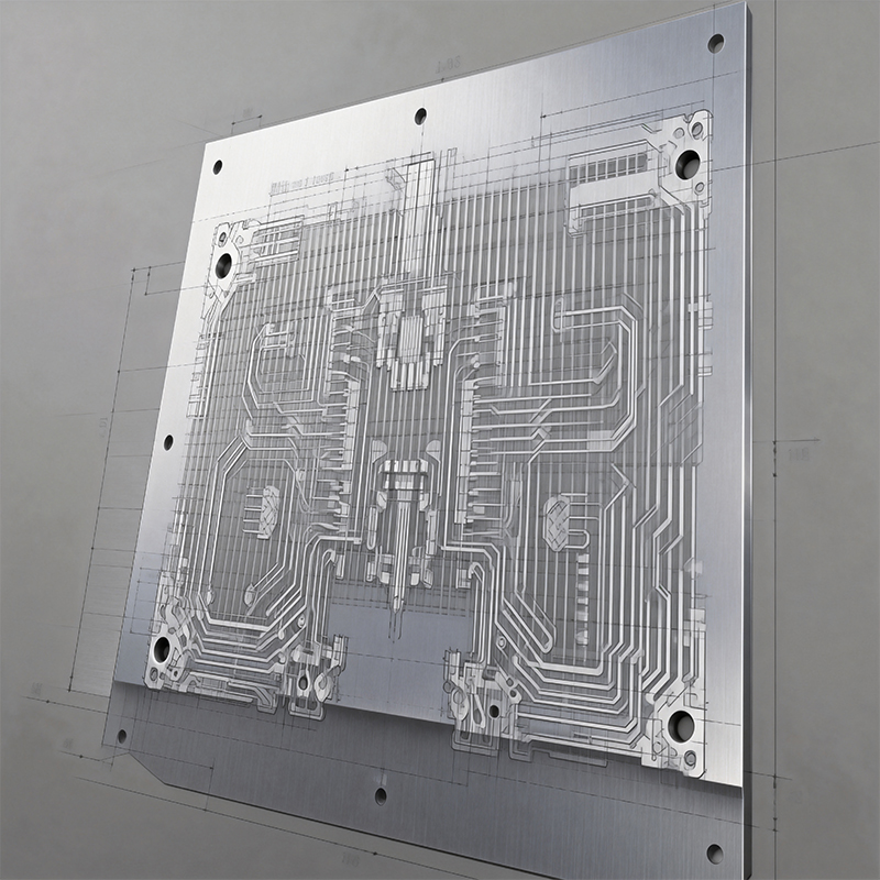
On the surface mount technology (SMT) production line, there’s a crucial tool that isn’t as eye-catching as the pick-and-place machine or reflow oven, yet it determines the very first step in the successful formation of thousands of micro solder joints. This is the PCB stencil—a thin stainless-steel sheet filled with precise apertures, acting as the indispensable “precision stamp” in the solder paste printing process.
Simply put, a stencil is a metal template with openings laser-cut at specific locations based on the circuit board design files. It has one core function: to accurately and uniformly “print” viscous solder paste onto every pad of the PCB that requires soldering, much like using a mold to make cookies. This lays the foundation for subsequent component placement and soldering. Without it, modern high-density electronic assembly would be nearly impossible.
The creation of a high-quality stencil relies on precision manufacturing technologies. There are three mainstream processes:
1. Laser-Cut Stencils
This is currently the most widely used and cost-effective technology. A high-energy laser beam directly ablates openings into a stainless-steel foil according to the design file. Its advantages are high precision, fast turnaround, and flexible modifications, making it ideal for most conventional PCB designs and the absolute industry standard.
2. Electroformed Stencils
This is an “additive” process. Nickel is electroplated onto a mandrel, gradually building up to form the stencil foil and create the apertures. Its characteristics are exceptionally smooth aperture walls, a natural trapezoidal cross-section (beneficial for release), and the ability to have locally varying thickness. These stencils offer long life and excellent printing performance but come with higher cost and lead time. They are typically used for applications with ultra-fine-pitch components (e.g., BGAs below 0.3mm pitch) or special requirements.
3. Hybrid/Enhanced Stencils
To balance cost and performance, hybrid processes exist. The most common is laser-cutting followed by electro-polishing. A chemical process smoothes the micro-roughness and burrs left by laser cutting, resulting in smoother aperture walls that reduce paste sticking and improve release. This is a highly practical enhanced solution.
A stencil is not a one-size-fits-all commodity; its parameters must be customized for the specific PCB design. Several key decisions directly impact final print quality:
1. Stencil Thickness is Fundamental
Thickness determines the volume of solder paste deposited. Common thicknesses are 0.1mm (4 mil), 0.12mm (4.7 mil), 0.13mm (5 mil), and 0.15mm (6 mil). The general rule: the finer the component pitch, the more precise the paste volume needs to be, requiring a thinner stencil. For large pads or power components needing more solder, local thickening or a step stencil might be necessary.
2. Aperture Design is an Art
Aperture size and shape are not simply a 1:1 copy of the pad. They are optimized based on component type, pad layout, and process experience:
Solder BGA Prevention: For chip resistors and capacitors, inverting the rectangular openings or creating a concave shape can effectively reduce solder balls formed during reflow.
Fine-Pitch Apertures: For chips with dense leads, a trapezoidal cross-section (top smaller than bottom or vice versa) is often used to improve paste release.
Large Pad Segmentation: Large ground or thermal pads are divided into multiple smaller grids to prevent excessive solder paste from causing component “floatation” or poor wetting.
3. Step Stencils and Nano-Coatings
Step Stencils: Using chemical etching or laser welding techniques on the same stencil foil to create areas of different thicknesses. This allows precise control over paste volume for different components.
Nano-Coatings: Applying an ultra-thin, smooth coating (e.g., Teflon-based) to the stencil surface. This significantly reduces solder paste adhesion and residue, further enhancing release quality and cleaning efficiency.
A stencil’s effectiveness spans its entire production life. Correct use and maintenance are critical:
Alignment and Framing: The stencil must be precisely aligned to the PCB’s fiducial marks using a vision system, often requiring accuracy within ±25 microns.
Printing and Cleaning: During high-speed printing, paste can clog tiny apertures. Regular bottom-side cleaning (e.g., every 5-10 boards) with dedicated wipes and solvent is essential to keep apertures clear.
Inspection and Tension Management: The stencil foil must be tautly stretched on its frame to remain flat. Regular checks with a tension meter are needed; a loose stencil causes inconsistent printing and poor accuracy.
In summary, the PCB stencil is the bridge connecting PCB design data to the physical deposition of solder paste. Though it operates behind the scenes, every detail—from its material and thickness to its aperture design and manufacturing process—directly impacts the success of the solder paste print. This, in turn, ultimately determines the yield of the entire SMT assembly process. Understanding the basic principles and selection criteria of stencils helps engineers and buyers make informed decisions, laying a solid foundation for high-quality electronics manufacturing from the very source.
Kaboer manufacturing PCBs since 2009. Professional technology and high-precision Printed Circuit Boards involved in Medical, IOT, UAV, Aviation, Automotive, Aerospace, Industrial Control, Artificial Intelligence, Consumer Electronics etc..