
Date: 2026-07-09
You've definitely seen them before. Those shiny gold contacts along the edge of a RAM stick or graphics card. You slide the card into a slot on the motherboard, and your computer recognizes the new hardware. Those gold contacts are called gold fingers.
Gold fingers (also called edge connectors) are the gold-plated conductive pads along the connecting edge of a printed circuit board. They're not actual fingers — they're a row of gold-plated metal contacts that transmit signals between circuit boards. In this guide, I'll explain what gold fingers are, what they do, what types exist, how they're designed, and how they're manufactured. Plain English, no fluff.
Gold fingers are the gold-plated conductive pads along the edge of a PCB. When you insert the board into a corresponding slot on another device, the gold fingers make contact with the metal springs inside the slot, allowing signals and power to flow between the two boards.
Your computer's RAM sticks, graphics cards, sound cards, and network cards all use gold fingers. When you push a RAM stick into its slot and hear that satisfying "click," that's the gold fingers locking into place.
Gold fingers serve one primary purpose: connection. Because they're plug-and-play connectors, they need several key properties:
Excellent conductivity: Signals must pass through cleanly
Wear resistance: Repeated insertion and removal shouldn't wear them out
Oxidation and corrosion resistance: They must not rust or tarnish over time
Not all gold fingers are the same length. Based on shape and application, there are three main types:
1. Regular Gold Fingers (Flush Fingers)
All contacts are the same length, neatly aligned along the board edge. The most common type — used on graphics cards and network cards.
2. Staggered Gold Fingers
Contacts have different lengths — some longer, some shorter. Common on USB flash drives, memory cards, and card readers.
3. Segmented Gold Fingers
Contacts are divided into segments with gaps between them. Used for specialized connection requirements.
The "gold" in gold fingers isn't pure gold — it's hard gold, specifically a nickel barrier plus a cobalt-gold alloy structure.
A typical gold finger stack looks like this:
Copper base: The PCB's copper traces at the bottom
Nickel layer (3-6 microns): Plated over the copper as a barrier to prevent copper-gold diffusion
Hard gold layer: Plated over the nickel — typically 98% pure gold + 2% cobalt (or nickel)
Why hard gold instead of pure gold?
Pure gold is too soft — it would wear away after a few insertions. Hard gold, alloyed with cobalt, is much more durable and can survive tens of thousands of insertion cycles.
Why not use ENIG (Electroless Nickel Immersion Gold) for gold fingers?
ENIG is a common surface finish for PCB pads, but it's not suitable for gold fingers. ENIG uses soft gold, typically only 2-5 microinches thick — too thin and too soft for repeated insertion. Gold fingers require electroplated hard gold, typically 5-30 microinches (µin) thick.
IPC-6012 specifies that commercial-grade gold fingers typically require 10-30 microinches of gold thickness, while aerospace-grade requires ≥50 microinches.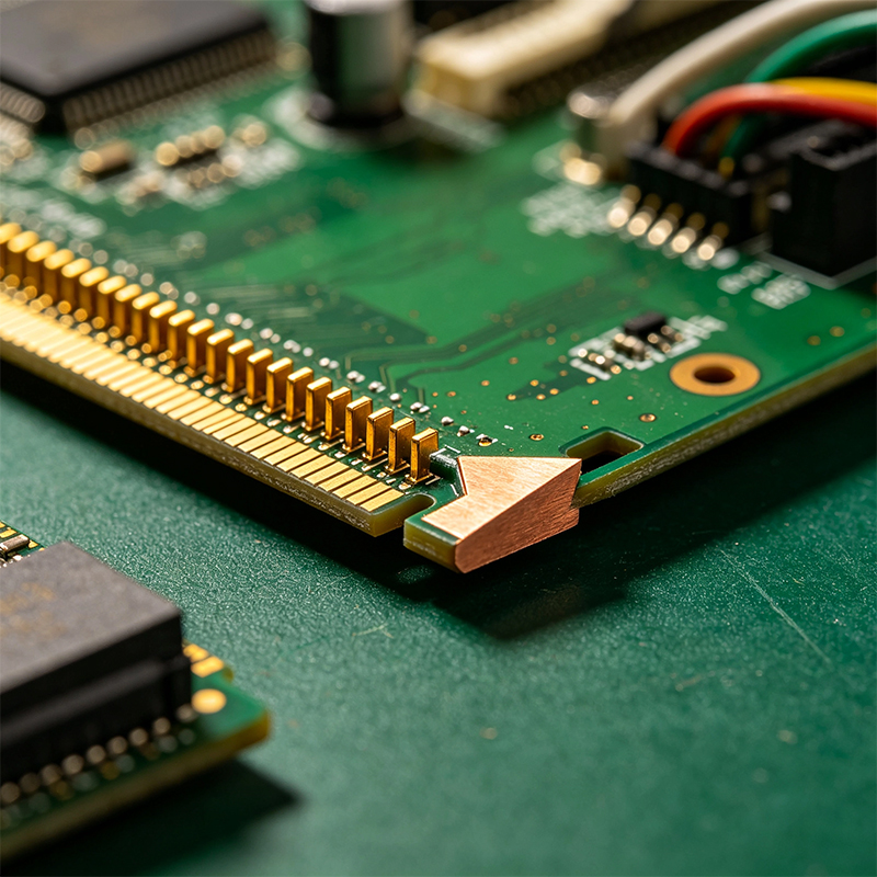
Gold finger manufacturing is more complex than standard PCB surface finishing. Key steps include:
Step 1: Electroplated Hard Gold
While regular PCB pads use ENIG, gold fingers must go through an electroplated hard gold process. The factory electroplates a 3-6 micron nickel layer on the finger area, then electroplates hard gold on top.
Step 2: Chamfering / Beveling
The board edge with gold fingers must be chamfered — ground down to an angle. The standard angle is 45 degrees, though 20 or 30 degrees are also used.
The chamfer serves one simple purpose: let the board slide smoothly into the slot. Without it, the board's square edge would slam into the connector springs, scraping the gold fingers and potentially damaging the slot.
Step 3: Solder Mask Opening
Gold finger areas must not be covered by any solder mask. If solder mask covers them, it would flake off during insertion and cause poor contact. All gold finger areas require a full opening window.
Step 4: Inner Layer Copper Pull-Back
The copper planes beneath the gold fingers must be pulled back — typically at least 3mm. This prevents uneven current distribution during electroplating and prevents exposed copper shorts during edge cutting.
If you're designing hardware, keep these rules in mind:
1. Gold Fingers Must Be at the Board Edge and Chamfered
Gold fingers must be designed at the board edge, and the manufacturer must be able to chamfer them. If the board is too small (under 5×5cm), chamfering may not be possible.
Chamfer depth also matters. For a standard 1.6mm thick board, the distance from the board edge to the gold finger must be at least 0.6mm. If the distance is too short, the chamfer will cut into the gold fingers.
2. Keep 1mm Clear Around Gold Fingers
Within 1mm of the gold fingers, no vias, SMD pads, or silkscreen should be placed. These would interfere with electrical performance or mechanical strength.
3. No Copper Pour on the Gold Finger Surface
Don't pour copper on the gold finger surface. If multiple fingers are connected by a copper pour, insertion will be difficult.
4. Gold Finger Areas Must Be Opened
Solder mask must not cover gold fingers. They must be fully exposed copper, ready for gold plating.
5. Minimum Board Size
A single board or panel with gold fingers must not be smaller than 50mm. Smaller boards are too difficult for the manufacturing equipment to handle.
Gold fingers are far more common than you might think:
Computer Hardware: RAM sticks, graphics cards, sound cards, network cards — all plug into motherboards via gold fingers
Storage Devices: USB flash drives, SSDs, memory cards
Telecom Equipment: Module boards in switches and routers
Industrial Equipment: Modular control boards that need frequent insertion
Consumer Electronics: Modular connections inside smartphones and smartwatches
Simply put: if it's a modular board that gets plugged and unplugged frequently, it probably uses gold fingers.
Gold fingers are the gold-plated conductive pads along the edge of a circuit board. They're made with electroplated hard gold (nickel barrier + cobalt-gold alloy) — wear-resistant, conductive, oxidation-proof, and built for thousands of insertion cycles. They come in regular, staggered, and segmented types. Design rules require 45-degree chamfering, solder mask opening, and inner layer copper pull-back. RAM sticks, graphics cards, USB drives, SSDs — gold fingers are inside devices you use every day.

Kaboer manufacturing PCBs since 2009. Professional technology and high-precision Printed Circuit Boards involved in Medical, IOT, UAV, Aviation, Automotive, Aerospace, Industrial Control, Artificial Intelligence, Consumer Electronics etc..


 English



 Wechat
 +86 13670210335
 +86 13670210335
 E-mail