
Date: 2026-07-27
You've definitely seen it in factory videos. A machine with several thin metal needles rapidly tapping on a circuit board, making a "tick tick tick" sound — like acupuncture for electronics. The probes move, touch, lift, and move again in a seamless, automated dance, testing a board in seconds.
Those flying needles are called the flying probe test.
Flying Probe Test (FPT) is an automated electrical testing method that uses movable probes to check the electrical integrity of a circuit board. No custom test fixtures required — the probes move according to a computer program, contacting test points one by one to check for opens, shorts, and component values. In this guide, I'll explain what flying probe testing is, how it works, and how it compares to traditional testing methods. Plain English, no fluff.
Flying probe testing uses 2 to 8 freely movable probes that, under computer control, "fly" across the PCB surface, sequentially contacting pads, vias, and component leads to perform electrical measurements.
Think of it as a robotic hand holding a multimeter probe, touching one point at a time across the board. Except this "robotic hand" is extremely fast — moving dozens of times per second with micron-level precision.
The key advantage: no test fixture required. Traditional testing requires a custom "bed of nails" fixture for each board, costing thousands to tens of thousands of dollars and taking weeks to build. Flying probe testing generates a test program directly from your design files — no fixtures, no waiting.
The process has three main steps:
Step 1: Generate the test program
The PCB design files (Gerber or CAD) are loaded into the flying probe tester. The machine automatically extracts all nets and test points, generating a complete test program. This step is fully automated.
Step 2: Place the board
The board is placed on the tester's worktable. Flying probe testing works on bare boards (no components) as well as PCBAs (fully assembled boards).
Step 3: Probes "fly" and test
Following the program, the probes move to each test point in sequence — touch, measure, lift, move to the next. The entire process is fully automated.
A typical flying probe tester has 2 to 8 probes, operating from both the top and bottom of the board simultaneously. More probes mean faster testing.
Flying probe testing catches a wide range of electrical defects:
Opens: broken traces that stop signals
Shorts: unintended connections between traces
Incorrect resistance: wrong resistor values
Incorrect capacitance: wrong capacitor values
Polarity errors: diodes, LEDs, or other polarized components installed backwards
Micro-shorts: tiny leakage between traces
Whether bare board or PCBA, flying probe testing covers most electrical defects.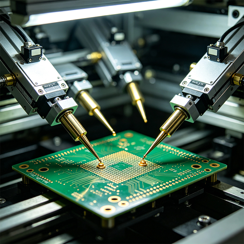
1. No fixtures — saves money
Traditional ICT requires a custom "bed of nails" fixture costing thousands to tens of thousands of dollars, with a 4-6 week development cycle. Flying probe testing generates a test program directly from your design files — zero fixture cost, zero waiting time.
2. Flexible — perfect for high-mix, low-volume
Switching boards on a flying probe tester just means loading a different program — no hardware changes needed. If you have 10 different board types with only a few dozen units each, flying probe testing is the most cost-effective option.
3. High precision
Flying probe probes can accurately contact extremely small pads and fine-pitch component leads with micron-level precision. For high-density, fine-pitch boards, flying probe testing outperforms traditional testing.
4. Fast setup
From design files to first test, flying probe testing typically takes hours to a day. Traditional ICT fixture development takes weeks.
1. Slow test speed
Probes move one point at a time — test time scales linearly with the number of test points. A complex board may take 5 to 15 minutes, with large boards exceeding 30 minutes. ICT completes the same test in seconds.
2. Not suitable for high-volume production
Due to its slow speed, flying probe testing isn't viable for high-volume production. If you're manufacturing tens of thousands of boards per month, you need ICT.
3. Limited functional test coverage
Flying probe testing covers electrical parameters, but it can't test full board functionality under real operating conditions — that requires Functional Circuit Test (FCT).
This is the most common comparison in PCB testing:
| Feature | Flying Probe Test (FPT) | ICT (In-Circuit Test) |
|---|---|---|
| Probe count | 2-8 movable probes | Hundreds to thousands of fixed probes |
| Fixture | None required | Custom bed-of-nails fixture — expensive, slow |
| Speed | Slow (5-30 min/board) | Very fast (seconds/board) |
| Flexibility | Very high — just change the program | Low — board change = fixture change |
| Best for | Prototypes, low-volume, high-mix | High-volume production |
In short: prototypes and low volume → flying probe test. High-volume production → ICT.
Flying probe testing is one of the fastest-growing segments in PCB testing. Two main drivers:
First, product lifecycles are shrinking.
New products come and go faster than ever — a product might only be in production for a few months before being replaced. Traditional ICT fixture costs and development cycles simply can't keep up. Flying probe testing's zero-fixture, fast-startup advantage fits this new reality perfectly.
Second, boards are getting more complex.
High-density boards, fine-pitch components, rigid-flex boards — these new PCBs are increasingly difficult to test with traditional bed-of-nails fixtures. Flying probe testing's flexibility and precision make it the ideal solution.
Flying probe testing is an automated electrical test method that uses movable probes to check circuit boards.
Its biggest advantage is no test fixtures required — saving time, saving money, and providing unmatched flexibility. It's best suited for prototype validation, low-volume production, and high-mix board types.
Its biggest disadvantage is slow test speed — not suitable for high-volume production, where ICT remains the standard.
Flying probe testing and ICT aren't competing technologies — they complement each other. Prototypes and low volume → flying probe test. High-volume production → ICT. Together, they provide complete PCB test coverage.

Kaboer manufacturing PCBs since 2009. Professional technology and high-precision Printed Circuit Boards involved in Medical, IOT, UAV, Aviation, Automotive, Aerospace, Industrial Control, Artificial Intelligence, Consumer Electronics etc..


 English



 Wechat
 +86 13670210335
 +86 13670210335
 E-mail