
Date: 2026-07-07
You've definitely seen them. Those white letters, boxes, and symbols on a green circuit board. "R1," "C2," little plus signs, company logos. These white markings are called the PCB silkscreen layer [6†L7-L9].
It's usually printed on the top and bottom layers of a board, typically in white ink. Its job isn't to conduct electricity — it's to tell people what's on the board, how to assemble it, how to test it, and how to repair it [1†L5-L6]. In this guide, I'll explain what the PCB silkscreen layer is, what it does, how it's printed, and what to watch out for when designing it [6†L20-L23].
The silkscreen layer (also called the legend layer) is the outermost layer of text, symbols, and graphics printed on a PCB [6†L4-L6][6†L11-L13]. It's those white letters, outlines, and logos you see on the board [0†L5-L6].
It's non-conductive — completely different from copper traces and solder mask [9†L14-L15]. Its purpose is to provide information — telling assembly workers where components go, which direction they face, and which pin is pin 1 [0†L7-L9][0†L11-L12].
Silkscreen is usually white because white contrasts best against the classic green solder mask [7†L13-L14]. But if the board has a white solder mask, the silkscreen is printed in black [1†L20].
The silkscreen layer does a lot more than just "look good" [9†L4-L5]. Here are its main jobs [10†L14-L16]:
1. Component Identification
This is the most basic job. Every component has a reference designator — "R1" for resistor 1, "C2" for capacitor 2, "U3" for IC 3 [0†L18-L20]. Without these labels, assembly workers wouldn't know which part goes where [1†L6].
2. Polarity and Pin 1 Indicators
Diodes, LEDs, and electrolytic capacitors have positive and negative terminals. ICs have pin 1. The silkscreen uses plus signs, dots, and corner marks to show orientation [11†L23-L24]. Install a component backwards, and the board might burn out.
3. Test Point Labels
Pads specifically designed for measuring signals are marked "TP1," "TP2," and so on [11†L30-L31]. Engineers know exactly where to probe during debugging [8†L4-L6].
4. Logos and Version Numbers
Many boards include company names, logos, board part numbers, revision numbers, and manufacturing dates [11†L33-L34]. These help with traceability if something goes wrong [3†L6-L7].
5. Safety Warnings
Some components get hot. The silkscreen warns with symbols like "high temperature" or "ESD sensitive" [9†L35-L36][11†L32].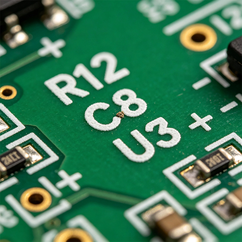
6. Assembly and Repair Guidance
Assembly operators follow the silkscreen to place components. Repair technicians follow it to find components. Without it, a bare PCB is unreadable [0†L38-L40].
It used to be printed with actual silk screens — that's where the name comes from [7†L14-L15]. Today, there are three main methods [10†L23-L24]:
Method 1: Manual Screen Printing
The traditional method. Epoxy ink is pushed through a nylon mesh stencil with a squeegee. Only for small runs with low precision requirements — line width typically >0.178mm [10†L25-L27].
Method 2: LPI (Liquid Photo Imaging)
This is the industry standard for modern production [10†L37-L38]. A liquid photo-sensitive epoxy ink is applied to the board (about 20-30μm thick), exposed to UV light through a photomask, unexposed ink is washed away, and finally cured at high temperature [2†L6-L8][10†L39-L46]. High precision — line width down to 0.15mm, character height down to 0.8mm [10†L48-L49].
Method 3: DLP (Direct Legend Printing)
Inkjet printers apply ink directly onto the board [9†L26-L27]. High precision, fast, good for dense boards [11†L17-L20]. Uses acrylic ink [2†L18].
Silkscreen may look simple, but bad design causes serious problems [8†L10-L24]. Here are the core rules [13†L5-L6]:
1. Don't Cover Pads
Silkscreen ink doesn't conduct electricity. If it covers a pad, components won't solder properly [5†L30-L32]. Minimum clearance from pads is typically 0.2mm [5†L36-L37].
2. Text Can't Be Too Small
IPC standards require character height of at least 0.8mm and line width of at least 0.15mm [3†L13-L15][13†L7-L13]. Too small, and the text becomes unreadable.
3. Good Contrast Is Essential
White ink on green solder mask is the classic combination [7†L13-L14]. If the board has a white solder mask, use black ink [1†L20]. Poor contrast makes text unreadable [9†L13-L14].
4. Keep Orientation Consistent
All text should face the same direction — either all horizontal or all vertical [11†L45-L48]. Mixing directions confuses assembly workers.
5. Don't Print Under Components
Text under a component gets covered up after assembly. It's a waste of ink [5†L10-L12].
These two layers are often confused [4†L21-L23]:
| Feature | Silkscreen | Solder Mask |
|---|---|---|
| Position | Outermost layer | Over copper traces |
| Color | Usually white | Usually green |
| Conductive? | No | No |
| Purpose | Provides information | Protects copper, prevents solder bridging |
Solder mask protects the board. Silkscreen tells people how to use the board [4†L11-L14].
The PCB silkscreen layer is the outermost layer of text and graphics on a circuit board.
It's non-conductive and provides information — where components go, their orientation, test points, version numbers. It's usually printed in white ink on top of the solder mask. Modern PCBs use LPI (Liquid Photo Imaging) for silkscreen printing.
Without the silkscreen layer, a circuit board is just a maze of copper and pads — assembly workers can't place parts, engineers can't test, and repair technicians can't fix. It doesn't carry current, but without it, the board is basically useless.

Kaboer manufacturing PCBs since 2009. Professional technology and high-precision Printed Circuit Boards involved in Medical, IOT, UAV, Aviation, Automotive, Aerospace, Industrial Control, Artificial Intelligence, Consumer Electronics etc..


 English



 Wechat
 +86 13670210335
 +86 13670210335
 E-mail