Date: 2025-12-31
Introduction
Look inside almost any electronic device made in the last 30 years—a smartphone, a laptop, a smartwatch. You’ll see a green board covered with tiny, flat rectangles and cylinders, looking almost like a miniature city. This isn’t an accident; it’s the result of Surface Mount Technology, or SMT. If you design, source, or manufacture electronics, understanding SMT isn’t just technical trivia; it’s key to building better, smaller, and more reliable products. Let’s break it down.
Part 1: SMT in Simple Words – From “Through-Hole” to “Surface Mount”
Before SMT, components had wire legs that were pushed through holes in the circuit board and soldered underneath (Through-Hole Technology). It was like building with Lego bricks that needed pegs to stick.
SMT changed everything. Surface Mount Technology is a method where components (called SMDs – Surface Mount Devices) are placed directly onto the surface of a printed circuit board (PCB) and soldered there. No holes needed for the components.
Think of it this way:
Through-Hole (Old Way): Plugging in Lego bricks.
SMT (Modern Way): Sticking flat stickers onto a page. It’s faster, allows for much smaller parts, and can be done with high-speed machines.
This shift enabled the electronics revolution, making devices smaller, faster to produce, and more affordable.
Part 2: How Does SMT Work? A Walk Down the Assembly Line
A modern SMT line is a symphony of precision machines. Here’s what happens to your PCB:
Solder Paste Printing: First, a stencil aligns over the PCB. Solder paste (a sticky mix of tiny solder balls and flux) is squeezed through, depositing precise dots of “glue” only where components will sit.
Component Placement: This is the star of the show. A pick-and-place machine uses a robotic nozzle to pick components from reels or trays. Guided by high-speed cameras, it places them onto the solder paste dots with incredible speed and accuracy—thousands of parts per hour.
Reflow Soldering: The board then travels through an oven called a reflow oven. The heat melts the solder paste, which flows to form a permanent electrical and mechanical bond as it cools. Creating the right temperature profile here is a science in itself.
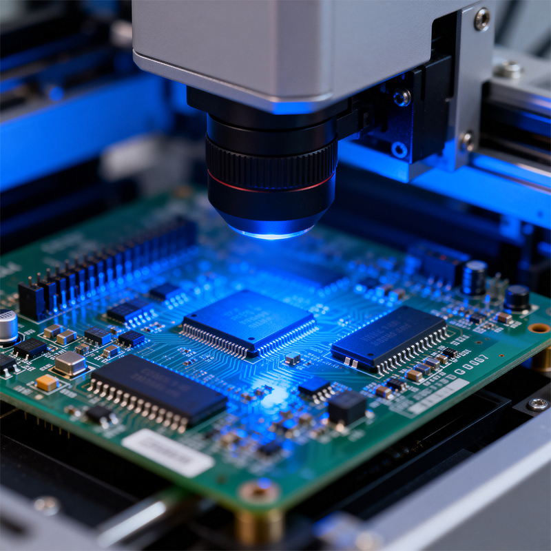
Inspection & Cleaning: After soldering, machines like Automated Optical Inspection (AOI) scan the board for defects: missing parts, misalignment, or bad solder joints. The board is then cleaned to remove any residue.

Part 3: Why SMT is Everywhere: Key Benefits for Your Product
Miniaturization: SMD components can be up to 10x smaller than through-hole parts, enabling complex devices in tiny forms (e.g., wireless earbuds).
Higher Performance: Shorter electrical paths allow for faster signal speeds and reduced interference.
Cost-Effectiveness: High-speed automation allows for massive-scale production at a lower cost per unit.
Design Flexibility: Components can be placed on both sides of the board, enabling more complex and dense circuit designs.
Part 4: The Real Challenge – It’s More Than Just Machines
While the process seems straightforward, achieving consistent, high-yield SMT assembly requires deep expertise:
Process Engineering: Dialing in the perfect stencil design, solder paste chemistry, and reflow profile for each unique board.
Supply Chain Mastery: Managing hundreds of miniature component reels and ensuring their quality.
Quality at Scale: Implementing robust inspection at every stage to catch defects before they become failures.
This is where partnering with an expert manufacturer becomes a strategic advantage, turning the complexity of SMT into a reliable foundation for your product.
Why Expertise in SMT Matters: A Glimpse into Kaboer’s Capabilities
At Kaboer, based in Shenzhen, China, we’ve built our PCBA service around mastering SMT. We understand that your success depends on flawless execution of this core technology.
Our dedicated SMT factory is equipped to handle the full spectrum of challenges:
Advanced & Agile Production Lines: We operate a mix of high-speed and ultra-precision placement machines. This allows us to efficiently handle both large-volume orders and complex, low-to-medium volume projects with fine-pitch components (like advanced BGAs or 0201 chips).
Process Control, Not Just Assembly: We invest in the process science. From SPI (Solder Paste Inspection) to post-reflow AOI, we use in-line data to monitor and control quality in real-time, aiming for exceptional first-pass yields.
Design for Manufacturing (DFM) Support: Our engineers work proactively. By reviewing your designs early, we can suggest optimizations for component layout or pad design to ensure the smoothest, most reliable SMT assembly possible.
The Shenzhen Advantage: Our location in the heart of the global electronics ecosystem provides unmatched agility in sourcing components and resolving supply chain issues swiftly, keeping your project on track.
Conclusion
Surface Mount Technology is the invisible, precision backbone of modern electronics. Understanding it helps you make better decisions. But harnessing its full potential requires a partner with the right equipment, expertise, and process discipline.
For electronics manufacturers looking for a reliable, expert extension of their team in Asia, Kaboer offers precisely that—turning the complexities of SMT into a straightforward path to a high-quality finished product.
Kaboer manufacturing PCBs since 2009. Professional technology and high-precision Printed Circuit Boards involved in Medical, IOT, UAV, Aviation, Automotive, Aerospace, Industrial Control, Artificial Intelligence, Consumer Electronics etc..