Date: 2026-01-30
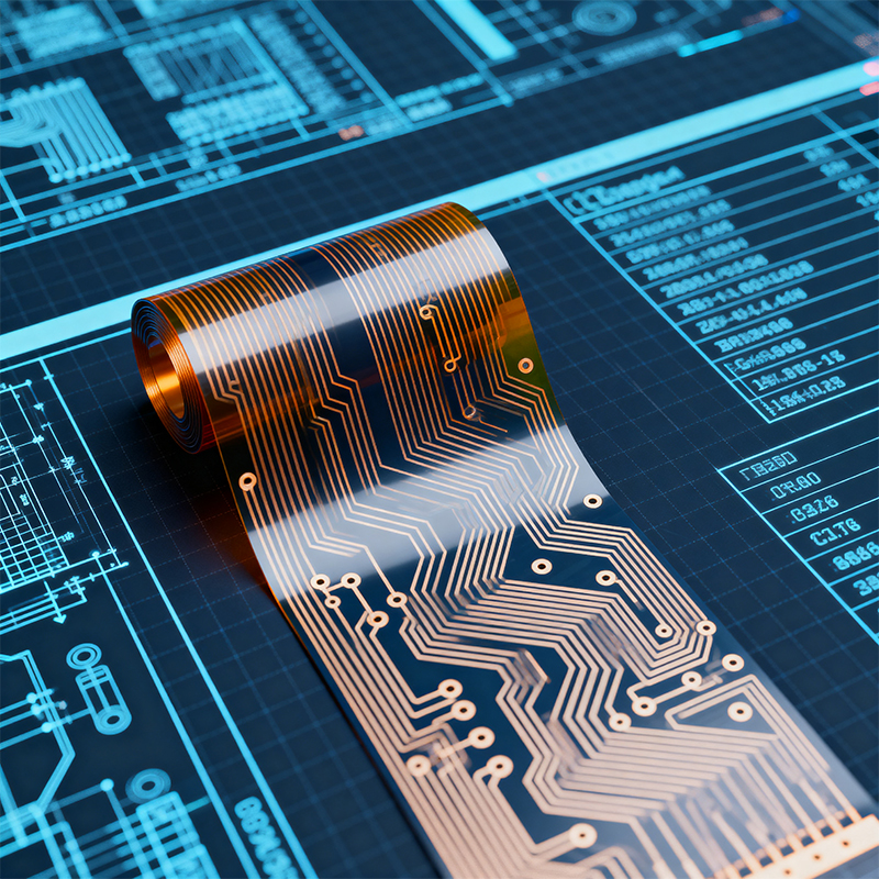
In modern electronics, flexible circuit boards (Flex PCBs) are the backbone of devices that need to bend, fold, or save space. From the hinge connectors in foldable smartphones to the internal wiring of smartwatches, and the precise components in automotive cameras and medical probes, this technology is indispensable. Unlike rigid PCBs, Flex PCB production is an ultimate test of precision, material science, and process control. Here is a detailed breakdown of its core production workflow.
| Stage | Key Processes | Core Objective & Explanation |
|---|---|---|
| Stage 1: Design & Material Prep | 1. Flex Circuit Design | Special layout in CAD software, focusing on trace routing, bend radius, and stress relief structures in dynamic flex areas. |
| 2. Substrate & Coverlay Selection | Substrate: Primarily Polyimide (PI) Film, valued for its high-temperature resistance, tensile strength, and excellent flex endurance. Conductor: Often uses Rolled Annealed Copper Foil (not Electro-Deposited) for its better grain structure suited for bending. Coverlay: Adhesive-coated PI film for insulation and outer layer protection. | |
| Stage 2: Patterning & Inner Layer Processing | 3. Patterning (Photolithography) | Laminating a photosensitive dry film onto the copper, then using UV exposure and development to transfer the circuit pattern onto the film, creating an etch resist. |
| 4. Precision Etching | Chemical solution removes unprotected copper, forming the fine copper trace pattern. The dry film is then stripped away. | |
| 5. Coverlay Lamination | Pre-punched coverlay film is precisely aligned and laminated onto the circuit layer under heat and pressure. | |
| Stage 3: Via Formation | 6. Drilling & Plating | Micro-vias are drilled using high-precision mechanical drills or UV/CO2 lasers. The walls are then metallized with copper via chemical deposition and electroplating to create interlayer connections. |
| Stage 4: Finishing & Rigorous Testing | 7. Surface Finish | Apply coatings like ENIG, Immersion Tin, or OSP to exposed pads for solderability, oxidation resistance, and contact reliability. |
| 8. Outline Profiling | Use precision die-cutting or laser cutting to separate the panels into the final, often irregular or dynamic, shapes. | |
| 9. Comprehensive Testing | Electrical Test: 100% check for opens/shorts. AOI: Scan for circuit defects. Critical Flex Testing: Repeated bending to simulate real use and validate lifespan/reliability. |
Industry Trend: The Potential of Additive Manufacturing
Beyond the mainstream "subtractive" etching process, the industry is exploring Printed Electronics. This additive approach uses inkjet or screen printing to deposit conductive inks or functional materials directly onto flexible substrates. It can significantly reduce material waste and chemical etching steps, offering a more sustainable and rapid manufacturing path for specific flexible electronic applications.
A high-quality Flex PCB is just the beginning. For electronics manufacturers, the real value lies in accurately and reliably integrating this flexible board with components to form a complete functional module or subsystem. This integration poses higher demands:
Design for Manufacturing Collaboration: A capable manufacturer provides early DFM feedback, optimizing your flex layout, component selection, and assembly strategy to de-risk the project from the start.
Precision Assembly Challenges: High-density SMT assembly on thin, flexible substrates requires unique solutions for board support, thermal management, and placement accuracy.
Testing Complexity: Functional testing may need to be performed in a flexed state, requiring customized test fixtures and programming.

Navigating the full-chain challenges from Flex PCB production to system integration requires an experienced, fully-capable partner. Shenzhen Kaboer Technology Co., Ltd. (Kaboer) is precisely that partner.
With our own advanced PCBA factory in Shenzhen, the heart of global electronics manufacturing, we specialize in flexible circuits and are dedicated to providing customers with a true turnkey solution—from Flex/Rigid-Flex PCB fabrication, component sourcing, and challenging SMT assembly to final functional testing.
How Kaboer Adds Value to Your Project:
End-to-End Control & Collaboration: We bridge the gap between flex fabrication and assembly, ensuring design intent is accurately executed at every step for seamless integration.
Proprietary Process & Technical Expertise: We possess proven experience in multilayer flex, high-reliability rigid-flex boards, fine-line circuitry, and precision component placement on flexible substrates.
Reliability-Centric Quality System: From raw material control to in-process monitoring and final dynamic flex endurance testing, we have a complete reliability validation process to ensure long-term performance in your end product.
When your innovative design calls for flexible electronics technology, Kaboer is ready to be your solid support. We deliver not just circuit boards, but a comprehensive manufacturing solution to bring your product vision to life.
Kaboer manufacturing PCBs since 2009. Professional technology and high-precision Printed Circuit Boards involved in Medical, IOT, UAV, Aviation, Automotive, Aerospace, Industrial Control, Artificial Intelligence, Consumer Electronics etc..