Date: 2026-01-30
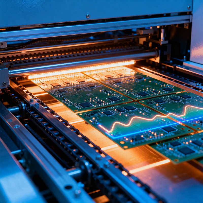
When you open any modern electronic device—be it a smartphone, computer, or smart appliance—you'll see a green circuit board densely populated with tiny black chips and components. Most of these components are not installed using traditional "through-hole soldering." Instead, they are "placed" and "bonded" onto the board surface through a precise process known as Surface Mount Technology. This is the essence of SMT assembly or processing.
In simple terms, SMT is the entire process of automatically and precisely placing miniature electronic components onto the surface of a printed circuit board (PCB) and permanently fixing them through reflow soldering. It is not "machining" in the traditional sense but a highly automated electronic assembly technology.
Before SMT became widespread, components had long leads that needed to be inserted through holes in the PCB and soldered on the opposite side. Here’s a quick comparison:
| Feature | Surface Mount Technology (SMT) | Traditional Through-Hole Technology (THT) |
|---|---|---|
| Component Mounting | Mounted on the surface of the PCB | Leads inserted through holes in the PCB |
| Component Size | Very small, thin, no long leads | Relatively larger, with long leads |
| Assembly Density | Extremely high, both sides can be used, enabling miniaturization | Lower, typically assembled on one side only |
| Automation Level | Fully automated, high-speed placement (tens of thousands of components per hour) | Lower automation, some manual insertion required |
| Typical Applications | Vast majority of modern consumer electronics, communication devices | High-power, high mechanical stress, prototyping scenarios |
It is precisely the advantages of miniaturization, high speed, and low cost brought by SMT that have made it the absolute mainstream in today's electronics manufacturing.
A complete SMT production line operates like a precision electronic assembly conveyor, consisting of the following core steps:
1. Solder Paste Printing: Preparing the "Electronic Glue"
What happens: A stencil with cut-out patterns is aligned over the PCB's pads. Like applying putty, a squeegee blade spreads solder paste (a paste containing tiny solder spheres and flux) through the stencil openings, depositing it precisely onto each pad that needs to be soldered.
Why it matters: This is the first step determining solder quality. The amount of paste deposited must be uniform and precise—too much can cause shorts, too little can lead to weak solder joints.
2. Component Placement: High-Speed, Precision "Micro-Placement"
What happens: The PCB with printed paste moves to the pick-and-place machine. Following pre-programmed coordinates, the machine's high-speed placement head picks up tiny resistors, capacitors, chips, etc., from reels, trays, or tubes and places them with astonishing accuracy (within ±0.05mm or better) onto their corresponding paste locations.
Why it matters: This is the core of SMT automation. Speed and accuracy directly determine production efficiency and yield.
3. Reflow Soldering: Making Components "Grow" onto the Board
What happens: The populated PCB enters a reflow oven. The oven has precisely controlled temperature zones. The solder paste goes through preheating, soaking, reflow (melting), and cooling stages. In the reflow zone, the paste melts, and due to surface tension and flux action, forms solid, shiny alloy solder joints between the component leads and PCB pads.
Why it matters: This is the key physico-chemical process creating reliable electrical and mechanical connections. Incorrect temperature profiles can lead to defects like cold joints, voids, or component damage.
4. Inspection & Testing: The "Quality Inspectors" Ensuring Perfection
What happens: After soldering, the PCB undergoes a series of checks:
Automated Optical Inspection (AOI): High-resolution cameras scan the board for missing, misplaced, wrong, or mis-oriented components.
X-Ray Inspection: Used to inspect solder joint quality under chips (like BGAs) that are invisible to the naked eye, detecting bridges or voids.
In-Circuit Test (ICT) / Functional Test (FCT): Electrical performance and functionality are verified via test probes or interfaces.
Why it matters: Detecting and eliminating defects early is crucial for ensuring final product quality.

5. Post-Processes (If Required): Completing the Board
If the design includes components that cannot be handled by SMT (like large connectors, transformers), they are added at this stage via selective wave soldering or hand soldering. Final steps may include protective conformal coating or potting.
While the SMT process seems standardized, challenges multiply when your design involves ultra-small components, flexible PCBs, rigid-flex boards, or high-density chips. A tiny error can cause an entire batch to fail.
This is where a partner with deep process expertise and end-to-end control becomes critical. This is the core value Shenzhen Kaboer Technology (Kaboer) provides.
As a professional manufacturer with its own advanced PCBA factory in Shenzhen, Kaboer doesn't just "run" an SMT line; we deepen our process expertise to tackle high-difficulty assembly challenges:
Full-Process Collaboration Starting with DFM: Our engineers conduct thorough Design for Manufacturability analysis before production, offering optimization advice on component selection, layout, and pad design to improve yield from the start.
Expertise in High-Difficulty Assembly: We specialize in precision SMT assembly, including stable placement of 0402, 0201, and even smaller components, as well as high-accuracy placement on flexible and rigid-flex boards, effectively managing challenges like alignment and deformation caused by flexible substrates.
End-to-End Quality System: From incoming inspection and in-process SPC monitoring to final AOI and X-Ray inspection, we have established a complete quality control loop, ensuring every board delivered meets high standards.
Efficient One-Stop Service: From PCB procurement, component sourcing, SMT assembly to testing and packaging, we provide integrated one-stop services within our own factory, ensuring smooth communication and on-time delivery, allowing you to focus more on product design and marketing.
Choosing Kaboer means selecting not just a factory, but a manufacturing solutions partner that helps you reliably realize complex designs.
Kaboer manufacturing PCBs since 2009. Professional technology and high-precision Printed Circuit Boards involved in Medical, IOT, UAV, Aviation, Automotive, Aerospace, Industrial Control, Artificial Intelligence, Consumer Electronics etc..