Date: 2025-11-04
Let me walk you through how we turn raw materials into working circuit boards. I'll break it down so it actually makes sense.
Making the Bare PCB - The Foundation
Think of this like building the roads before any cars can drive on them.
First, we start with the base material - usually FR4 (that sturdy fiberglass stuff) or flexible polyimide for bendable boards. We take this blank canvas and cover it with copper everywhere.
Then comes the fun part - we transfer the circuit pattern onto the copper. It's like using a stencil: we protect the copper we want to keep and etch away everything else. What's left are those shiny copper traces you see on circuit boards.
Next, we drill holes - for components to go through, for mounting the board, and for connecting different layers in multi-layer boards.
After drilling, we add that green protective coating you're probably familiar with (though it can be other colors too). This solder mask keeps the copper from shorting out and getting damaged. Then we print the white labels that show where each component goes.
Finally, we coat the exposed copper with something like tin or gold to prevent corrosion and make soldering easier later.
The result? A bare PCB - ready for components but can't do anything useful yet.
Turning PCB into PCBA - Where the Magic Happens
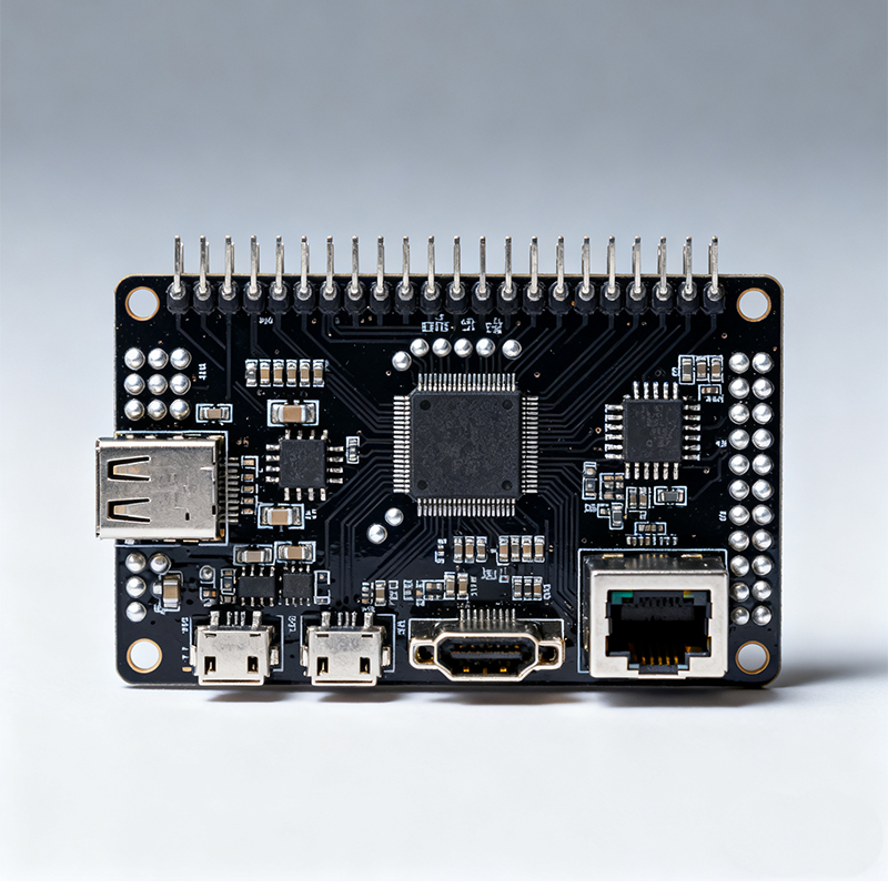
This is where we bring the board to life by adding all the electronic components.
First, we check that everything is up to spec - the bare boards, the resistors, chips, everything. No sense building with bad materials.
Then we program our pick-and-place machines. These robots are incredible - they can place dozens of components per second with amazing accuracy.
The assembly happens in two main ways:
For most small components (resistors, capacitors, chips), we use SMT (Surface Mount Technology). The machine places components directly onto the board's surface, then we run it through an oven that melts the solder to create permanent connections.
For larger components with wires or pins, we use through-hole technology. These components get inserted into drilled holes, then we wave-solder the bottom of the board to connect everything.
Testing - The Make-or-Break Phase
This is where we separate the working boards from the duds.
We start with visual checks - both automated (using camera systems) and manual inspection. We're looking for problems like bridges between pins, components that aren't properly seated, or soldering issues.
Then comes the real test - we power up the board and see if it actually works. Does it do what it's supposed to do? We test every function to make sure.
When we find problems (and we always find some), our repair team works their magic - reflowing solder, replacing components, fixing whatever's wrong.
Finally, we clean off any flux residue, package the good boards properly, and ship them out.
The Big Picture Difference
PCB manufacturing is about creating the platform
PCBA manufacturing is about populating that platform and making it functional
It's like the difference between building a house (PCB) and furnishing it with everything needed to live in it (PCBA). One is incomplete without the other.
I've seen plenty of customers get confused about this distinction. Just last week, we had someone order bare PCBs when they really needed fully assembled boards. They ended up with beautiful but useless boards that couldn't power on. That's why understanding this difference is so important - it saves time, money, and frustration.
Whether you need just the bare boards or complete assembled units, now you know what goes into making each one. And if you're ever unsure, just ask - we're happy to help you figure out what you actually need for your project.
Kaboer manufacturing PCBs since 2009. Professional technology and high-precision Printed Circuit Boards involved in Medical, IOT, UAV, Aviation, Automotive, Aerospace, Industrial Control, Artificial Intelligence, Consumer Electronics etc..