Date: 2026-02-02
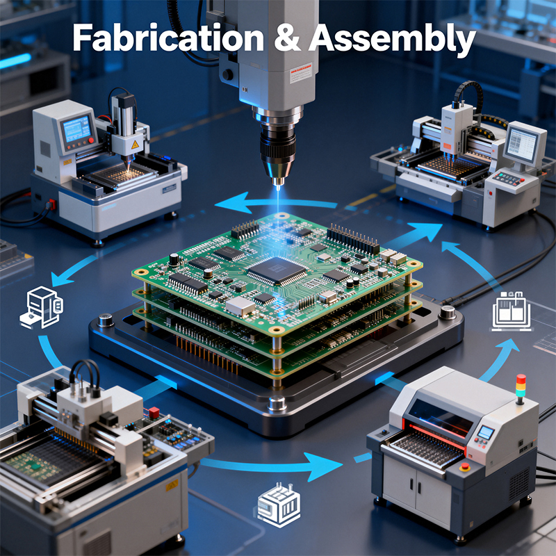
When you have a brilliant idea for an electronic device, how does it transform from a design on your computer into a working physical product in your hand? This transformation relies primarily on two core stages: PCB Fabrication and PCBA Assembly. They are the foundational steps in bringing electronic hardware to life. Understanding these stages helps you better plan projects, communicate with manufacturers, and appreciate the journey your product takes.
Simply put, fabrication is about creating the bare “canvas” (the blank PCB), while assembly is about “installing” various electronic components onto that canvas to give it full functionality. Let’s break down each step.
Imagine fabricating a circuit board as “etching” a complex network of copper roads onto an insulating substrate. Here are the key steps for a standard multilayer board:
Design & Output: Engineers finalize the PCB layout using specialized software and output the Gerber files (the “construction blueprints”) and drill files.
Inner Layer Imaging & Etching: Starting with copper-clad laminate, the circuit pattern is transferred onto the copper foil via photolithography. Chemicals then etch away the unwanted copper, leaving behind the precise traces.
Lamination: The etched inner layer cores, prepreg (bonding material), and copper foil are stacked like a “sandwich” and fused into a solid multilayer panel under high heat and pressure.
Drilling: Precision mechanical drills or lasers create holes in the panel for component leads and to interconnect layers (through-holes, blind/buried vias).
Hole Metallization & Plating: Through chemical deposition and electroplating, a conductive copper layer is deposited on the non-conductive hole walls, creating electrical connections between layers.
Outer Layer Patterning & Etching: A process similar to the inner layers is repeated to form the final outer layer traces and pads.
Solder Mask & Surface Finish: The green solder mask is applied (to prevent solder shorts), and exposed copper pads receive a finish like ENIG or HASL for solderability and oxidation resistance.
Silkscreen & Routing: White component identifiers and text are printed on the board. Finally, the individual boards are cut from the panel according to the outline file.
At this point, a shiny, intricate “canvas” is ready, awaiting its components.
The goal of assembly is to accurately place and securely attach hundreds or thousands of components like resistors, capacitors, and chips onto their designated locations on the bare board.
Solder Paste Printing: Using a stainless-steel stencil, viscous solder paste is precisely “squeegeed” onto all the PCB pads.
Component Placement: High-speed pick-and-place machines use nozzles to pick tiny components from reels and place them with incredible speed (tens of thousands per hour) and accuracy onto the pasted pads.
Reflow Soldering: The populated PCB travels through a reflow oven with a precisely controlled temperature profile. The solder paste melts, flows, and then solidifies, creating a permanent solder joint.
Through-Hole & Wave Soldering: Larger components not suitable for SMT (like some connectors) are inserted, and the board is passed over a wave of molten solder to form the connections.
Cleaning & Inspection: Flux residue is cleaned off. Automated Optical Inspection (AOI), X-ray, and other methods rigorously check solder quality, especially for hidden joints (e.g., under BGA chips).
Programming & Functional Testing: Microcontrollers are programmed with firmware, and the fully assembled board is powered up and tested to ensure it functions as designed.
To clearly distinguish the focus of each stage:
PCB Fabrication is about creating the platform: It deals with substrates, copper, and insulating materials. Its core process is subtractive manufacturing (removing copper by etching). Its output is the bare board.
PCBA Assembly is about integrating components: It deals with resistors, capacitors, ICs, and other discrete parts. Its core process is additive and joining (adding and soldering components). Its output is the functional module or finished board.
In practice, fabrication and assembly are tightly linked. Many manufacturers now offer “one-stop” services, managing the entire process from receiving your Gerber files and Bill of Materials (BOM) through to PCB fabrication, component sourcing, SMT assembly, and testing.
The advantages are clear: it simplifies your supply chain management, ensures process continuity, reduces the time and quality risks of shipping between separate factories, and can optimize overall cost through consolidated orders.
In conclusion, Fabrication and Assembly are two interlocking, highly specialized phases in the realization of electronic hardware. Understanding the complete journey from “blank canvas” to “intelligent module” is the essential first step to successfully turning any electronic idea into a reliable product.
Kaboer manufacturing PCBs since 2009. Professional technology and high-precision Printed Circuit Boards involved in Medical, IOT, UAV, Aviation, Automotive, Aerospace, Industrial Control, Artificial Intelligence, Consumer Electronics etc..