
Date: 2026-08-01
Your product is running at Gbps data rates — USB 3.0, PCIe Gen4, DDR5, 100G Ethernet. The moment the signals go high-speed, your board starts misbehaving. Eye diagrams close. Data jitters. EMI fails. Intermittent failures appear. You spent countless hours on circuit design, only to be stuck by the board itself.
That's the world of high-speed PCBs. It's not "faster" standard PCB — it's a completely different design philosophy. Materials, stackups, impedance, routing, manufacturing — every single aspect is different from standard boards.
The global high-speed PCB market was valued at $5.08 billion in 2025**, projected to reach **$5.96 billion in 2026 and $13.22 billion by 2031, growing at a staggering 17.28% CAGR. AI servers, 5G base stations, data centers, autonomous driving — almost every board in these sectors is a high-speed PCB.
In this guide, I'll explain what high-speed PCBs are, their core challenges, how to select materials, how to design them, and how they're manufactured. Plain English, no fluff.
First, let's get one thing straight: what does "high-speed" mean?
In PCB design, "high-speed" doesn't have a fixed frequency threshold. It means that the signal's rise time is short enough that PCB traces can no longer be treated as "wires" — they must be treated as "transmission lines".
When signal frequencies exceed a few hundred MHz and data rates exceed 1 Gbps, PCB traces stop behaving like simple wires. They become transmission lines. Impedance mismatch causes reflections. Long traces cause attenuation. Adjacent traces cause crosstalk. Discontinuous reference planes cause radiation. The "just connect the dots" logic of standard PCB design completely fails at high speeds.
High-speed PCB design is a process of balancing circuit design requirements, device technologies, and fabrication materials and methodologies, to deliver a PCB that can transfer signals between components with integrity.
High-speed PCB performance is 70% material, 30% process. Choose the wrong material, and no amount of routing will save you.
Standard FR4 becomes very lossy above 1-2GHz — its dissipation factor (Df) is around 0.015-0.020. High-speed PCBs need low-loss materials, with significantly lower Df.
Current mainstream low-loss materials include:
Panasonic Megtron series (Megtron 4/6/7) : Modified epoxy ultra-low-loss laminates that support both high-speed digital and high-frequency RF signals. Megtron 6 is widely used in 56G/112G networking, AI, and server applications.
Rogers series: Ceramic-filled PTFE or hydrocarbon substrates with stable Dk and extremely low Df, ideal for RF and mmWave applications.
Isola Tachyon series: For 56G/112G high-speed networks.
By choosing low-loss materials like Megtron 6 or Rogers, designers can achieve cleaner eye diagrams, support data rates up to 112G, and maintain better signal integrity.
For designs below 3GHz, standard FR4 is still sufficient. Above that, low-loss materials are essential. Many high-end designs use hybrid stackups — Rogers or Megtron for high-speed signal layers, FR4 for power and ground layers — balancing performance and cost.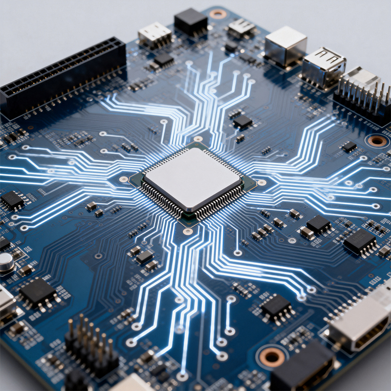
High-speed PCB design isn't just about making traces wider and spacing larger. It has its own complete set of rules.
1. Impedance Control
This is the single most important rule in high-speed PCB design. Every high-speed trace must have controlled characteristic impedance — common values are 50Ω single-ended, 90Ω differential (USB), 100Ω differential (HDMI/Ethernet) .
Impedance mismatch causes signal reflections — part of the signal energy "bounces back" and adds to the original, causing ringing, data jitter, and in severe cases, eye diagram closure. Impedance tolerance is typically ±10%, with high-end products requiring ±5% or better.
2. Continuous Reference Planes
Every high-speed signal trace must have a complete reference plane (ground or power) — and it must be continuous and unbroken. The reference plane is like the signal's mirror — the signal runs on the top trace, and the return current runs on the reference plane below. If the plane is split or broken by vias, the return current detours, loop area increases, and EMI gets worse.
3. Differential Pair Routing
USB, PCIe, HDMI, and Ethernet all use differential signals — two traces running together with signals as mirror images. Differential pairs require:
Impedance matching: Differential impedance controlled to specification (90Ω or 100Ω)
Length matching: Length difference between the two traces kept within 5 mils
Consistent spacing: Constant gap between the two traces
Symmetrical vias: Vias placed symmetrically
Differential pair imbalance is a common issue in high-speed PCB projects, often discovered only after prototype testing — a costly problem that can delay time-to-market.
4. Shortest Paths
High-speed signal traces should be as short as possible. Keep the distance between drivers and receivers minimal to reduce propagation delay and signal attenuation.
5. Avoid Stubs and Sharp Corners
Unnecessary stubs cause signal reflections. 90-degree corners cause signal reflections and EMI at high frequencies. Use 45-degree angles or curves for trace corners.
6. Via Control
Every via introduces parasitic capacitance and inductance — an impedance discontinuity point for high-speed signals. Minimize the number of vias on high-speed signal traces.
Good design is only half the story — you still have to manufacture it. High-speed PCB manufacturing is significantly harder than standard PCB manufacturing.
1. High Layer Counts, Complex Structures
AI server and telecom high-speed PCBs typically require 18+ layers with 4-8 step HDI structures. More layers mean harder lamination alignment — misregistration beyond 0.05mm means vias miss pads.
2. High Aspect Ratio Micro-hole Processing
High-speed PCBs demand increasingly high aspect ratios (board thickness ÷ hole diameter). Drilling these micro-holes presents real challenges — positioning accuracy, drill breakage, chip removal, tool wear, misalignment.
3. Consistent Impedance Control
High-speed PCB impedance tolerances are far tighter than standard boards — ±10% is the baseline, with ±5% or tighter for high-end products. Any deviation in trace width, dielectric thickness, or copper thickness during manufacturing can push impedance out of spec.
4. Difficult Material Processing
High-frequency low-loss materials (like PTFE-based Rogers) are soft and have high CTE, making drilling and lamination much harder than FR4.
5. DFM Check Must Be Front-Loaded
Late-stage discovery of manufacturing constraints remains one of the most common drivers of PCB program delays. High-speed PCB DFM checks must be done during design, not after boards are made.
High-speed PCBs are used wherever "standard boards can't handle it":
AI Servers: AI compute boards demand extreme routing density and signal integrity.
5G Communications: 5G base stations and mmWave antennas need low-loss materials and high-frequency performance.
Data Centers and High-Speed Networks: 56G/112G backplanes, high-speed switches, optical modules.
Automotive Electronics: ADAS, automotive radar, autonomous driving compute platforms.
Consumer Electronics: Flagship smartphones, tablets, gaming consoles.
Test and Measurement: High-speed oscilloscopes, spectrum analyzers, signal generators.
The global high-speed PCB market is growing at an astonishing rate. The market was valued at $5.08 billion in 2025**, projected to reach **$5.96 billion in 2026 and $13.22 billion by 2031** — a **17.28% CAGR**. The high-frequency high-speed board market was valued at **$3.82 billion in 2025, projected to reach $13.84 billion by 2035 at a 13.74% CAGR.
AI servers, 5G infrastructure, and autonomous driving are the three core growth drivers.
We are not a standard rigid-only PCB shop. We are a one-stop manufacturer that designs and makes flexible PCBs, rigid-flex boards, HDI high-frequency boards, and then does full PCBA. High-speed PCBs are one of our core capabilities.
All in-house: PCB fabrication, SMT, DIP, inspection, and assembly under one roof. Every step is under our control.
High-frequency low-loss material experience: Megtron 4/6/7, Rogers (RO4000/RO3000 series), PTFE, LCP — we've done them all.
High-precision manufacturing: Minimum trace/space 0.05mm, minimum laser blind via 0.075mm. Supports 1-order to any-layer HDI, up to 20+ layers.
Impedance control precision: Impedance tolerance down to ±5%, meeting the tight requirements of high-speed signals.
Signal integrity support: We step in during the design phase — stackup design, impedance calculation, differential pair optimization — ensuring signal quality from the start.
High-speed testing capability: Equipped with TDR (Time Domain Reflectometry) and other high-speed test equipment to verify actual impedance and signal quality.
IPC-compliant: Fabrication and inspection to IPC-6012, IPC-A-610, and IPC-J-STD-001 — Class 2 and 3.
Free DFM review: Send your design files, get a DFM report within 24 hours — including material selection, stackup design, impedance control, and manufacturability assessment.
Three simple steps:
Send your files: Gerbers, BOM, stackup and impedance requirements, target data rates.
We review and quote: Within 24 hours, you'll receive a DFM report, material recommendations, and sample/volume pricing.
Sample, then scale: We build samples. You test signal integrity and functionality. Then we move to volume.
High-speed PCBs aren't "more expensive standard boards" — they're a completely different design philosophy and manufacturing process. The global high-speed PCB market is growing at over 17% CAGR, and AI and 5G are turning high-speed PCBs from a "high-end option" into an "industry standard."
If you're designing a product that runs high-speed signals, send us your requirements. We won't push a contract — we'll first run a free DFM review and material recommendation, and let our expertise speak.
When you contact us, please include:
Product type and application (AI server, 5G, ADAS, data center, etc.)
Target data rates and interface types (PCIe, USB, DDR, Ethernet, etc.)
Estimated annual quantity (samples, small batch, or mass production)
We'll give you an honest answer — what we can do, what we can't, and how to modify your design to make it work

Kaboer manufacturing PCBs since 2009. Professional technology and high-precision Printed Circuit Boards involved in Medical, IOT, UAV, Aviation, Automotive, Aerospace, Industrial Control, Artificial Intelligence, Consumer Electronics etc..


 English



 Wechat
 +86 13670210335
 +86 13670210335
 E-mail