
Date: 2026-08-01
You've definitely seen the hair‑thin copper traces on a circuit board. But have you ever wondered how those traces are actually “drawn” onto the board? Copper foil starts out as a solid sheet covering the entire board — how do you remove the unwanted copper and leave only the traces?
The answer lies in a material that looks like “blue plastic wrap” — dry film photoresist.
Dry film photoresist (DFR) is one of the most critical materials in PCB manufacturing. Without it, those dense, precise circuit patterns simply couldn't be made. In this guide, I'll explain what dry film photoresist is, how it works, and where it's used. Plain English, no fluff.
Dry film photoresist is simply a light‑sensitive polymer film. It comes on rolls like plastic wrap, typically colored blue or purple. It's a three‑layer sandwich:
Top layer: A protective polyester film that keeps the photoresist clean and scratch‑free
Middle layer: The actual photosensitive polymer layer — this is what reacts to light
Bottom layer: A peelable cover sheet, removed before use
Unlike liquid photoresist (which is sprayed or brushed on like paint), dry film photoresist is a solid film that's applied to the board surface using heat and pressure. Think of it like ironing plastic wrap onto the board — except this “plastic wrap” reacts to light.
The principle is simple: light hardens it; unexposed areas wash away.
The process has four steps:
Step 1: Lamination
The dry film photoresist is pressed onto the copper surface using heated rollers. Temperature, pressure, and speed must be precisely controlled — a poor lamination ruins everything downstream.
Step 2: Exposure
The board is placed under UV light. A photomask (like a film negative) blocks light where it's not wanted, allowing UV to hit only the areas that should become circuit traces. Where the light hits, the photoresist undergoes a chemical reaction and hardens.
Step 3: Development
The board goes into a developer solution. Unexposed photoresist dissolves away, exposing the copper underneath. The exposed (hardened) photoresist stays in place, protecting the copper from being etched.
Step 4: Etching or Plating
Now the copper has a protective “mask” — hardened photoresist covers the traces, while bare copper is etched away or plated with other metals. Finally, the photoresist is stripped off, leaving behind the precise copper circuit pattern.
Dry film photoresist became the industry standard for good reasons:
1. Uniform Thickness
Dry film is factory‑made with consistent thickness. Liquid photoresist, applied by spraying or rolling, is much harder to keep uniform.
2. Clean Operation
Dry film is a solid sheet — you just laminate it on. Liquid photoresist involves spraying and volatile solvents, making a much messier operation.
3. Good Adhesion
Laminated with heat and pressure, dry film photoresist provides more consistent and reliable adhesion than liquid coatings.
4. High Yield
Compared to liquid photoresists, dry film processes are more stable with fewer defects, resulting in higher yields.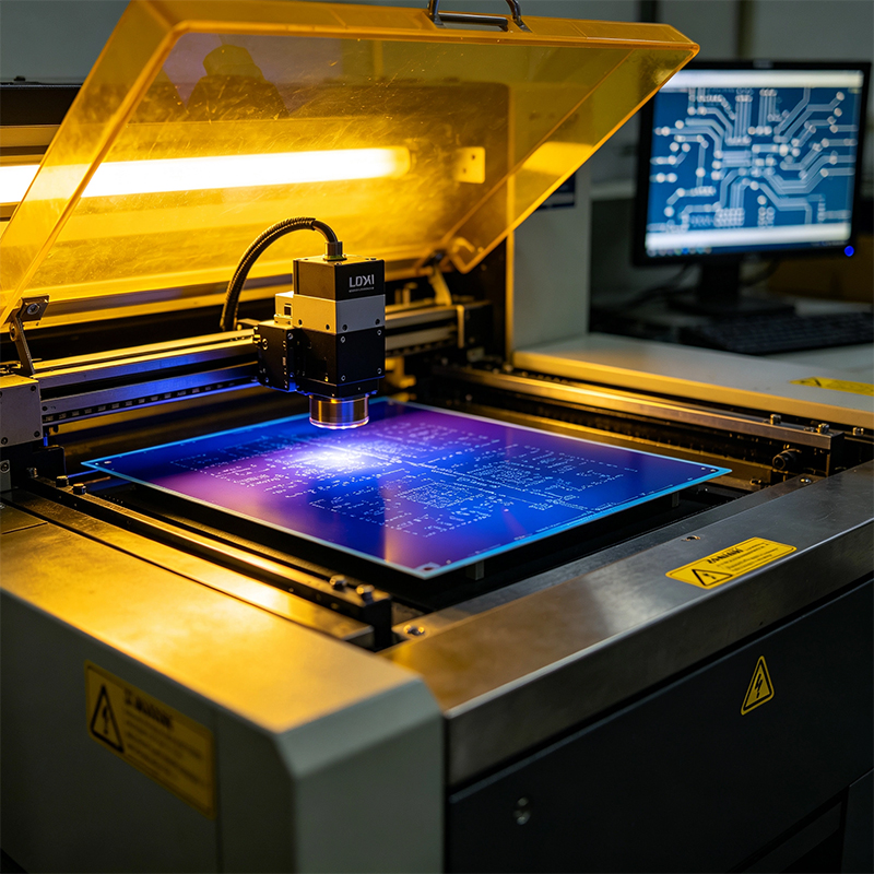
5. Suitable for Automated High‑Volume Production
Lamination, exposure, and development can all be automated — making dry film photoresist ideal for large‑scale PCB manufacturing.
Many people confuse the two. Here's a quick comparison:
| Feature | Dry Film Photoresist | Liquid Photoresist |
|---|---|---|
| Form | Solid film on a roll | Liquid, like paint |
| Application | Heat‑pressed lamination | Spray, roller, or curtain coating |
| Thickness control | Very uniform | Uneven, varies with coating conditions |
| Work environment | Clean, minimal fumes | Solvent fumes, needs ventilation |
| Best for | High‑volume PCB production | Specialty boards, thick boards, fine lines (<30μm) |
| Resolution | Down to 15μm line/space | Higher resolution for ultra‑fine lines |
Simply put: dry film is laminated on — uniform, clean, great for high volume. Liquid is applied — flexible but harder to control.
Dry film photoresist is used across a wide range of applications:
Rigid PCBs: Computer motherboards, phone boards, power supplies
Flexible PCBs (FPC) : Wearable devices, foldable display cables
Rigid‑Flex Boards: Drones, medical endoscopes
HDI Boards: 5G base stations, AI servers
IC Substrates and Packaging: Chip packaging, advanced packaging
MEMS Devices: Micro‑electromechanical systems
Lead Frames: Semiconductor packaging
Demand for dry film photoresist in advanced packaging is particularly strong — AI server chip packaging is driving rapid growth in this market. Major global manufacturers include Asahi Kasei, Eternal Materials, and Showa Denko Materials.
Dry film photoresist is a light‑sensitive solid film that creates precise circuit patterns on circuit boards through lamination, exposure, and development.
It's more uniform, cleaner, and better suited for high‑volume production than liquid photoresist. It's one of the most critical materials in PCB manufacturing — without it, those hair‑thin traces in your phone simply couldn't be made.

Kaboer manufacturing PCBs since 2009. Professional technology and high-precision Printed Circuit Boards involved in Medical, IOT, UAV, Aviation, Automotive, Aerospace, Industrial Control, Artificial Intelligence, Consumer Electronics etc..


 English



 Wechat
 +86 13670210335
 +86 13670210335
 E-mail