Date: 2026-02-06
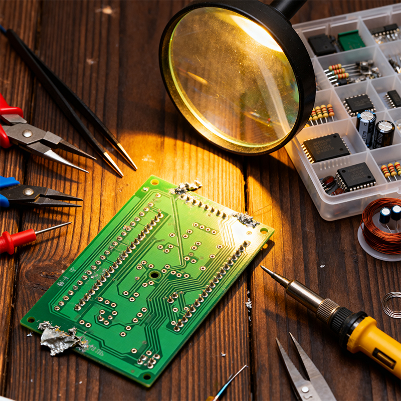
A custom-designed PCB for a smart beehive monitoring system, produced in a batch of just 30 pieces, is what connects a hobbyist beekeeper in California to a factory floor in Shenzhen.
The world of hobbyist electronics is booming. From custom drone flight controllers and retro game console mods to home automation systems and environmental sensors, creative individuals worldwide are turning ideas into tangible devices. At the heart of these innovations lies a critical component: the Printed Circuit Board (PCB).
Unlike mass-produced commercial electronics, hobbyist projects demand small-batch, high-mix manufacturing with a focus on flexibility, design support, and accessibility. For a maker, a single functional prototype can be the difference between a shelved idea and a successful Kickstarter campaign. This is where the journey of a hobby PCB begins.
What exactly is a "Hobby PCB"? It’s not defined by the technology itself, but by its purpose, scale, and the relationship between the creator and the manufacturer.
Commercial PCBs are driven by volume, rigorous cost-optimization, and long-term supply chain stability. Hobby PCBs, in contrast, are driven by experimentation, customization, and learning. The order quantity is typically small—anywhere from 5 to 100 pieces. The priority isn't the lowest cost per unit at a scale of 10,000, but rather the highest chance of success for a first-time prototype.
These projects often involve novel form factors or integrations that aren't found in off-the-shelf products. This is where advanced technologies like Flexible PCBs (for wearables or compact devices) and Rigid-Flex PCBs (for moving parts like robotic arms or custom cameras) become highly relevant, even for non-commercial projects.
The path from a design software like KiCad or Altium to a working board in hand is fraught with potential pitfalls for hobbyists.
The most common challenge is Design for Manufacturability (DFM). A design might look perfect on screen but contain features that are impossible or excessively costly to produce. This includes traces that are too thin, holes placed too close to edges, or a lack of proper clearances. Without DFM feedback, a creator might receive unusable boards, wasting both time and budget.
Furthermore, material and technology selection can be daunting. Does your high-frequency radio module require a specific high-frequency laminate for stable performance? Does your compact design need HDI (High-Density Interconnect) techniques with laser-drilled micro-vias? Most hobbyists lack the practical experience to make these calls, leading to under- or over-specifying their boards.
For over a decade, Kaboer has operated at the intersection of professional manufacturing and accessible prototyping. Based in Shenzhen, the heart of global electronics innovation, we understand that behind every small-batch order is a passionate creator with a vision.
We bridge the gap between hobbyist innovation and industrial-grade quality. Our core offerings—Flexible PCBs, Rigid-Flex Boards, and HDI High-Speed/High-Frequency PCBs—are precisely the technologies that enable cutting-edge hobbyist projects. Whether you’re building a flexible circuit for an e-textile project or a complex 6-layer HDI board for a custom compute module, we have the in-house expertise and equipment to realize it.
What truly sets a professional partner apart for a hobbyist? It's the support structure that de-risks the entire process.
First, we offer complimentary preliminary DFM checks. Before your board goes into production, our engineers review your files for common issues, providing feedback that can prevent costly mistakes. For more complex projects, we offer deeper design consultation services, advising on stack-up, impedance control, and thermal management.
Second, we treat every order with professional rigor, regardless of quantity. Your batch of 20 boards undergoes the same controlled processes, testing protocols (like Electrical Testing and Flying Probe), and quality inspections as an order of 2,000. This ensures the reliability of your prototype is not compromised.
We believe trust is built on transparency. This is why we actively encourage and welcome our clients—including hobbyists and small startups—to visit our PCBA factory in Shenzhen.
A factory tour allows you to see the precision behind your boards: the laser direct imaging for fine traces, the automated optical inspection (AOI) systems, and the skilled technicians performing assembly. It demystifies the process and builds confidence in the partnership. For our international friends who cannot travel, we facilitate virtual tours and live video calls with our engineering team to discuss your project in detail.
Many iconic products began as hobby projects. When your prototype is successful and you’re considering a small production run for a community sale or a crowdfunding campaign, Kaboer is positioned to scale with you.
We provide a seamless transition from prototype to low-volume production, ensuring design consistency and component sourcing support. Our team can advise on design optimizations for better cost-effectiveness at scale and guide you on compliance and certification pathways relevant to your market.
The next wave of electronic innovation often starts not in corporate R&D labs, but in garages, workshops, and home offices. At Kaboer, we are passionate about empowering that innovation. We provide the professional manufacturing backbone that allows creative minds to focus on what they do best: designing, experimenting, and inventing.
By choosing a partner who understands both the technology and the unique needs of the maker community, you transform your hobby PCB from a simple circuit into a reliable foundation for your ideas.
Kaboer manufacturing PCBs since 2009. Professional technology and high-precision Printed Circuit Boards involved in Medical, IOT, UAV, Aviation, Automotive, Aerospace, Industrial Control, Artificial Intelligence, Consumer Electronics etc..