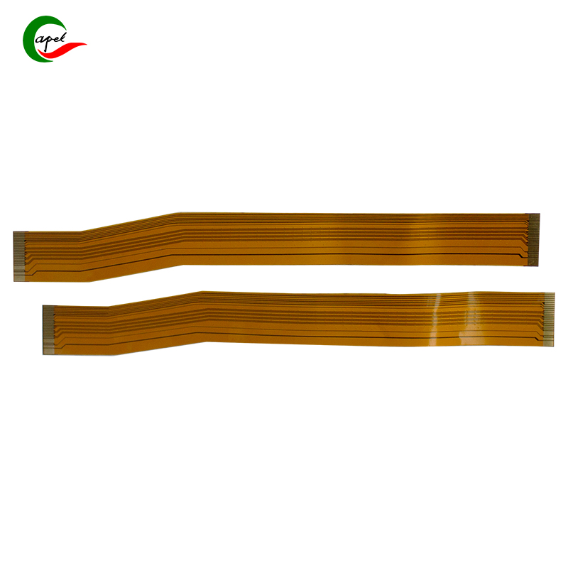
Imagine a PCB factory discarding 15% of its raw materials—copper sheets, polyimide films, solder paste—every month. For a mid-sized manufacturer, that’s $50,000 in wasted resources annually, not to mention the environmental harm (e.g., discarded copper ending up in landfills). In FPC/PCB production, material waste isn’t just a financial hit—it’s a sustainability failure.
FPCs and PCBs rely on costly, finite materials: copper (for traces), polyimide (for flexible layers), and FR4 (for rigid boards). Waste often comes from poor design (e.g., oversized boards), inefficient cutting, or unused scraps. The good news? Simple, actionable changes can cut waste by 30% or more. Below are 4 proven strategies, backed by real factory examples.
One of the biggest waste culprits is "dead space"—unused areas on a PCB/FPC panel. For example, a designer might leave large gaps between circuits, or use an oversized board when a smaller one works. To fix this:
- Panelization Software: Use tools like Altium or KiCad to "nest" multiple small boards on a single panel (e.g., fitting 20 smartwatch FPCs on one polyimide sheet instead of 15). A Chinese FPC maker did this and cut material use by 22% in 3 months.
- Standardize Sizes: Avoid custom board sizes that force factories to cut odd shapes (which create more scraps). A European PCB firm switched to 3 standard panel sizes and reduced scrap waste by 18%.
Every square millimeter of unused space is wasted material—optimizing design turns that space into usable product.
Cutting and etching (removing excess copper) are critical steps—and major sources of waste if done poorly. Here’s how to fix it:
- Laser Cutting for FPCs: Traditional die-cutting for FPCs leaves 10-15% scrap. Laser cutting is 3x more precise, trimming scrap to just 3-5%. A U.S. wearable tech supplier switched to laser cutting and saved 800kg of polyimide film yearly.
- Additive Etching for PCBs: Instead of etching away 70% of a copper sheet (standard subtractive etching), use additive etching—printing only the copper needed for traces. Samsung’s PCB plant adopted this and cut copper waste by 45%.
Precision tools don’t just reduce waste—they also improve product quality (e.g., cleaner cuts mean fewer defective boards).

Not all waste has to be thrown away. FPC/PCB scraps are rich in recyclable materials:
- Copper Recycling: Melt down copper scraps and repurpose them for new traces. A Japanese factory recycles 90% of its copper waste, saving $30,000 yearly and reducing reliance on new copper mining.
- Polyimide Reuse: Grind unused polyimide scraps into powder, mix with new resin, and make low-grade flexible layers (for non-critical parts like connectors). A Taiwanese FPC maker does this, cutting polyimide waste by 30%.
- Solder Paste Saving: Use automated dispensers to apply only the needed amount of solder paste (manual application wastes 20-30%). Also, collect unused paste, reprocess it, and reuse it for non-critical joints.
Recycling isn’t just eco-friendly—it’s profitable. The more you reuse, the less you spend on new materials.
Even the best tools fail if workers don’t know how to use them. Waste often comes from small, repeated mistakes:
- A worker cutting a panel slightly off-center, ruining the whole sheet.
- A designer ignoring panelization guidelines, creating extra scrap.
Fix this with training:
- Operator Training: Teach workers to calibrate cutting machines daily and spot early signs of waste (e.g., uneven etching). A Mexican PCB factory trained its team and reduced human-caused waste by 25%.
- Designer Workshops: Educate designers on "waste-minimizing design" (e.g., standard sizes, efficient nesting). A Canadian firm did this and saw design-related waste drop by 19%.
Waste prevention is a team effort—when everyone understands the cost of waste, they’ll take steps to avoid it.
Reducing FPC/PCB material waste isn’t just about "being green"—it’s about saving money, improving quality, and staying competitive. By optimizing design, using precision tools, recycling scrap, and training teams, you can turn waste into savings.
A mid-sized U.S. PCB factory adopted all 4 strategies and cut total material waste by 32% in one year—saving $65,000 and reducing its carbon footprint by 28%. The lesson? Waste isn’t inevitable—it’s a choice. And the choice to reduce it pays off for your budget and the planet.
Founded in 2009, our company has deep roots in the production of various circuit boards. We are dedicated to laying a solid electronic foundation and providing key support for the development of diverse industries.
Whether you are engaged in electronic manufacturing, smart device R&D, or any other field with circuit board needs, feel free to reach out to us via email at sales06@kbefpc.com. We look forward to addressing your inquiries, customizing solutions, and sincerely invite partners from all sectors to consult and collaborate, exploring new possibilities in the industry together.