Date: 2025-12-27
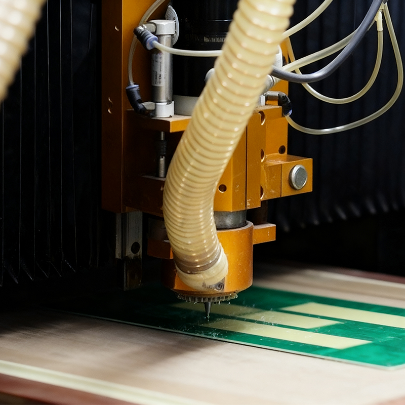
Milling a PCB board refers to the process of using a computer-controlled mechanical milling machine (a CNC router) with specialized miniature cutting tools to physically remove copper and substrate material from a copper-clad laminate. This creates isolated conductive traces, pads, and the board's physical outline. It is a subtractive, mechanical machining process that stands in contrast to the mainstream chemical etching method. PCB milling is primarily valued for rapid prototyping, producing custom one-off boards, and creating precise board outlines, slots, or cutouts that are challenging to achieve with standard panelized fabrication.
The process is analogous to a CNC machine carving a part from a solid block but executed on a microscopic scale suitable for electronics.
From Digital Design to Machine Instruction: A PCB layout file (typically Gerber or Excellon format) is imported into dedicated milling software. This software translates the design into precise tool paths—a set of coordinates and commands that dictate where and how deep the cutting tool should move.
Precision Material Removal: The machine uses a series of end mill bits:
A V-bit or engraving bit (with a 30-60 degree point) is used to "isolate" or "define" traces. It cuts narrow channels through the copper layer, removing material to electrically separate the desired circuit paths from the surrounding copper foil.
A flat end mill is used to drill holes (for vias and component leads) and to cut the final board outline from the larger substrate panel.
Sequential Fabrication: The machine executes the tool paths in sequence: 1) milling away copper to form the circuit pattern, 2) drilling all required holes, 3) cutting the completed board free from the waste material.
| Feature | PCB Milling (Mechanical) | Chemical Etching (Photolithographic) |
|---|---|---|
| Process Principle | Subtractive, mechanical material removal using a rotating cutter. | Subtractive, chemical dissolution of unwanted copper using an etchant solution. |
| Setup & Lead Time | Extremely fast for one-off prototypes. No chemical preparation, photographic masks, or UV exposure required. | Slower initial setup. Requires imaging (mask creation), photoresist application, exposure, and development prior to etching. |
| Materials & Waste | Uses standard FR-4 copper-clad laminate. Generates dry, solid waste (copper and fiberglass dust), which is easier to contain and dispose of. | Requires chemicals, photoresist, and water for rinsing. Generates hazardous liquid waste (spent etchant) requiring neutralization and specialized disposal. |
| Typical Resolution | Limited by the physical diameter of the cutting tool (typically down to ~0.2 mm trace/space). Accuracy can be affected by tool wear or deflection. | Very high resolution. Modern processes can reliably achieve trace/space below 0.1 mm (4 mil) and are essential for high-density designs. |
| Layer Capability | Most practical for 1 or 2 layers. Double-sided milling requires precise flipping and alignment, which is complex. Multi-layer boards are not feasible. | The standard for all multi-layer boards (from 2 to 50+ layers). Allows for reliable interlayer connections via plated through-holes. |
| Best Suited For | Rapid functional prototypes, RF/high-frequency boards (precise trace geometry), custom shapes/slots, and board modifications/rework. | All volume production and the only viable method for high-density interconnect (HDI), complex multi-layer boards, and large batch manufacturing. |
This technique excels in specific niches where its unique advantages are paramount:
In-House Rapid Prototyping: Enables an "idea-to-hardware" loop within hours. Engineers can design, mill, populate, and test a board in a single day, significantly accelerating R&D cycles.
RF and Microwave Circuit Prototypes: Milling produces traces with clean, vertical sidewalls. Unlike chemical etching, which can cause undercut (isotropic etching beneath the mask), milling preserves the exact designed trace width, which is critical for controlled impedance and predictable high-frequency performance.
Creating Complex Board Outlines, Slots, and Cutouts: This is a key strength. It can easily produce non-rectangular shapes, internal mounting holes, or precise edge connectors that would require additional and costly routing steps in a standard fabrication flow.
Modifications, Debugging, and Rework: A milling machine can be used as a precision tool to cut traces on an existing board for debugging, isolate faulty sections, or add modifications, saving a full board spin.

Not for Volume Production: It is a serial process—each trace is cut individually. This makes it economically impractical for producing more than a handful of identical boards.
Surface Finish and Features: Mill traces have a matte, textured finish compared to the smooth, plated surface of etched boards. It cannot create plated through-holes or apply solder mask and silkscreen—features standard in finished products.
Skill-Dependent Results: Success depends on operator skill for calibration, tool selection, and feed/speed settings. Improper setup can lead to broken tools or damaged boards.
Q1: Can a PCB milling machine create plated through-holes (PTH)?
A: No. A milling machine only drills holes. Plating through-holes requires a complex electrochemical deposition process (electroplating) conducted in a full-scale PCB fabrication facility with chemical baths.
Q2: What file formats are needed to run a PCB milling job?
A: The standard and most reliable inputs are Gerber files (RS-274X) for the copper layers and board outline, and an Excellon (NC Drill) file for hole locations and sizes. The milling software then converts these into machine-specific G-code.
Q3: Is a milled PCB suitable for a final product?
A: Almost never. Milling is unequivocally a prototyping and specialist fabrication method. Final products require the durability, consistency, plated holes, and professional soldermask/silkscreen finishes that only established chemical etching and manufacturing processes can provide reliably and at scale.
Q4: What are the main operational costs of PCB milling?
A: The primary costs are capital investment in the machine and consumable cutting bits, which wear and break. The cost per prototype for the raw blank PCB material is very low. There are no ongoing costs for chemicals, masks, or plating lines.
Kaboer manufacturing PCBs since 2009. Professional technology and high-precision Printed Circuit Boards involved in Medical, IOT, UAV, Aviation, Automotive, Aerospace, Industrial Control, Artificial Intelligence, Consumer Electronics etc..