Date: 2026-01-26
If you've ever wondered how today's smartphones can be so thin yet so powerful, or how complex industrial equipment manages to fit so much functionality into compact spaces, multilayer PCBs are a big part of the answer. Let's explore what makes these circuit boards special.
Beyond the Basic Board
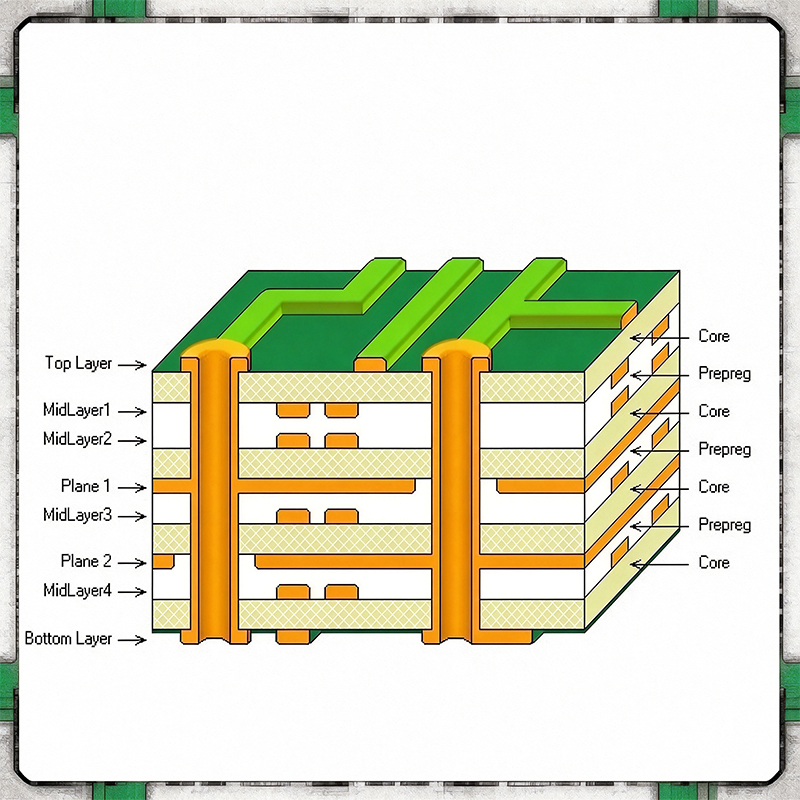
A regular PCB is like a single-floor house—everything happens on one level. A multilayer PCB, on the other hand, is more like an apartment building with multiple floors connected by internal hallways (called vias). These boards have several conductive copper layers sandwiched between insulating material, all laminated together into a single, unified board.
Why Go Multilayer?
Think about organizing a workshop. With only one workbench (a single-layer board), everything gets crowded quickly. Add multiple shelves and storage levels (additional layers), and suddenly you have space to organize tools, materials, and work areas efficiently. That's essentially what multilayer PCBs do for electronic circuits.
Common Configurations
4-layer PCBs: Very common—often used in consumer electronics.
6 to 8-layer PCBs: Found in more complex devices like networking equipment.
10+ layer PCBs: Used in high-performance computing, medical devices, and aerospace applications.
Some advanced boards can have 30, 40, or even more layers for extremely specialized applications.

Key Advantages for Manufacturers
Space Saving: The most obvious benefit. By building upward (adding layers) rather than outward, devices can be smaller and more compact.
Better Performance: Dedicated layers can be assigned for power and ground, reducing electrical noise and improving signal quality—crucial for high-speed circuits.
Increased Circuit Density: More connections can be made in the same footprint, enabling more complex functionality.
Enhanced Reliability: With careful design, multilayer construction can provide better heat distribution and structural strength than single-layer alternatives.
The Manufacturing Process (Simplified)
Creating multilayer PCBs is like preparing a sophisticated layered sandwich:
Individual thin layers are first etched with their circuit patterns.
These layers are stacked with insulating material between them.
The stack undergoes heat and pressure to bond everything together.
Holes are drilled and plated to create connections between layers.
Finally, outer layers are processed and finished like standard PCBs.
Design Considerations
Working with multilayer PCBs requires more planning upfront:
Careful layer arrangement (which signals go on which layers)
Strategic placement of vias (the "elevators" between layers)
Attention to heat management
More complex testing requirements
Real-World Applications
You'll find multilayer PCBs in:
Smartphones, tablets, and laptops
Automotive control systems
Medical imaging equipment
Industrial automation controllers
Telecommunications infrastructure
Aerospace and defense systems
When to Consider Multilayer Design
If your design involves high-speed signals, complex circuitry, space constraints, or sensitive components that need shielding from interference, multilayer PCBs are likely worth considering.
Just like cities build upward to maximize limited space, electronics use multilayer PCBs to pack more capability into smaller packages. This technology quietly enables the miniaturization and performance we've come to expect from modern electronics.
Kaboer manufacturing PCBs since 2009. Professional technology and high-precision Printed Circuit Boards involved in Medical, IOT, UAV, Aviation, Automotive, Aerospace, Industrial Control, Artificial Intelligence, Consumer Electronics etc..