
Date: 2026-07-28
If you’ve ever looked at a shiny metal part on a car, a connector inside your phone, or the gold pads on a circuit board, chances are there’s a thin layer of nickel underneath doing the heavy lifting. That layer didn’t get there by accident — it was put there through a process called nickel electroplating.
In this guide, I’ll walk you through what nickel electroplating is, how it actually works, why it’s used in so many industries (especially electronics), and what makes it different from other plating methods. No chemistry degree required — just plain talk about a process that quietly makes modern life possible.
Let’s start with the basics. Nickel electroplating is a process that uses electricity to deposit a thin, uniform layer of nickel metal onto the surface of a conductive object. Think of it like painting with metal — except instead of a brush, you’re using an electric current to move nickel ions from a solution onto the object you want to coat.
The object being plated becomes the cathode (the negative electrode), and a piece of nickel (or a nickel alloy) becomes the anode (the positive electrode). Both are submerged in a chemical bath called an electrolyte, which contains dissolved nickel salts. When you turn on the power, nickel ions from the solution are attracted to the cathode and deposit onto its surface as a solid metal layer.
It sounds complicated, but the basic idea is simple: electricity + chemicals + nickel = a protective metal coating that makes things last longer, work better, and look nicer.
Nickel isn’t just chosen at random. It has a combination of properties that make it ideal for electroplating:
Corrosion resistance — Nickel doesn’t rust or corrode easily. A nickel layer acts as a shield, protecting the underlying metal from moisture, chemicals, and the elements. This is why nickel plating is widely used in automotive parts, marine equipment, and outdoor hardware.
Hardness and wear resistance — Nickel is tough. It can withstand friction, abrasion, and mechanical stress much better than bare copper or aluminum. That makes it perfect for connectors, switches, and other parts that get handled or moved repeatedly.
Ductility — Nickel can bend and stretch without cracking. This might sound minor, but it’s crucial for parts that need to flex or expand and contract with temperature changes.
Adhesion — Nickel bonds well to other metals. It creates a strong, reliable foundation for additional coatings like gold, silver, or tin.
Solderability — Nickel provides an excellent surface for soldering. In PCB manufacturing, this is a big deal because it ensures components can be reliably attached to the board.
Barrier layer — Nickel stops metals from diffusing into each other. For example, in PCB manufacturing, a nickel layer prevents gold from migrating into copper — which would ruin the board.
In short, nickel does a lot of things well. It’s like the Swiss Army knife of metal coatings.
Let’s break down the process step by step. In a typical nickel electroplating setup, here’s what happens:
Before anything else, the object to be plated needs to be thoroughly cleaned. Any dirt, grease, oil, or oxide layer on the surface will prevent the nickel from sticking properly. Depending on the material, this might involve:
Degreasing — using solvents or alkaline cleaners to remove oils and grease
Acid etching — using mild acids to remove oxides and roughen the surface slightly for better adhesion
Rinsing — washing the object with water between each step to prevent contamination
Think of it like painting a wall — you wouldn’t paint over dirt and expect the paint to stick. Same principle here.
The clean object is immersed in a nickel electroplating bath. The bath contains:
Nickel salts (usually nickel sulfate and nickel chloride) — these provide the nickel ions that will deposit onto the object
Boric acid — this acts as a pH buffer, keeping the bath at the right acidity level for the process to work properly
Additives — various chemicals that control the brightness, smoothness, and stress level of the nickel deposit
The bath is carefully maintained at a specific temperature (usually around 50-60°C), pH level (typically 3.5-4.5), and chemical concentration. If any of these factors are off, the nickel layer won’t come out right.
The object to be plated is connected as the cathode (negative electrode), and a nickel anode is connected as the positive electrode. When the power supply is turned on:
Nickel ions (Ni²⁺) in the solution are attracted to the cathode (the object)
At the cathode, these ions gain electrons and become neutral nickel atoms, which deposit onto the surface as a solid metal layer
At the anode, nickel metal dissolves into the solution as ions, replenishing the bath
The longer the current runs, the thicker the nickel layer becomes. Typical thicknesses in PCB applications range from 2.5 to 5 micrometers, though thicker coatings are used for other applications.
After the desired thickness is achieved, the plated object is removed from the bath and rinsed thoroughly to remove any residual chemicals. It’s then dried, and the process is complete.
In some cases, the nickel layer may receive additional treatment — like heat treatment to improve adhesion, or a top coat of gold, silver, or tin for enhanced performance.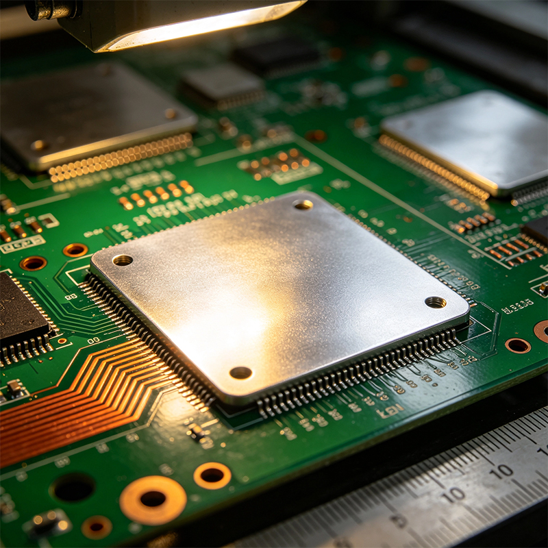
There are actually two different ways to deposit nickel onto a surface. They’re often confused with each other, but they work quite differently:
This is the method I’ve been describing — it uses an external electrical current to drive the deposition. The object must be conductive (metal) to be plated this way.
Pros:
Faster and cheaper for high-volume production
Can achieve 100% pure nickel deposits
Thicker coatings are possible
Cons:
Uneven coating thickness — edges and corners get thicker deposits
Requires complex fixturing for oddly shaped parts
Limited to conductive materials
This method uses a chemical reaction rather than electricity to deposit nickel. No external current is needed. The bath contains a reducing agent (usually sodium hypophosphite) that triggers the deposition chemically.
Pros:
Uniform thickness even on complex shapes and internal surfaces
Works on non-conductive materials (with proper preparation)
Superior corrosion and wear resistance
Lower porosity than electrolytic coatings
Cons:
More expensive
Slower process
Contains phosphorus (typically 3-10%), which makes it less electrically conductive
Not as durable or wear-resistant as electrolytic nickel
Both methods have their place. Electrolytic nickel is used when you need pure nickel, thick coatings, or low cost. Electroless nickel is used when you need uniform coverage, complex shapes, or superior corrosion resistance.
This is where nickel electroplating really shines — and where it’s probably most relevant to you if you work with electronics.
In PCB (printed circuit board) manufacturing, nickel is used as an underlayer beneath other surface finishes like gold or silver. Here’s why:
It acts as a barrier. Copper and gold don’t play nicely together. Over time, gold atoms will diffuse into copper, causing the joint to become brittle and unreliable. A nickel layer between them prevents this migration completely.
It prevents oxidation. Copper oxidizes when exposed to air, which makes it hard to solder. Nickel doesn’t oxidize as easily, so it keeps the surface solderable.
It provides a strong base. Nickel bonds well to both copper and gold. It creates a reliable foundation for the gold layer that actually makes contact with components.
It extends shelf life. PCBs with nickel plating can sit in storage for months without the pads becoming unsolderable. This is a huge advantage for manufacturers who need to keep inventory.
The most common PCB finish that uses nickel is ENIG — Electroless Nickel Immersion Gold. This is the gold-colored pad you see on most high-quality circuit boards. Underneath that thin gold layer is a thicker layer of nickel, and underneath that is the copper trace.
Another increasingly popular finish is ENEPIG — Electroless Nickel Electroless Palladium Immersion Gold. This adds a palladium layer between the nickel and gold for even better reliability, especially in demanding applications like automotive and aerospace.
Typical nickel thickness in PCB applications is around 4 to 5 micrometers, though it can range from 2.5 to over 10 micrometers depending on the requirements.
Nickel plating is everywhere. Here are some of the most common places you’ll find it:
Gold pads on circuit boards (ENIG)
Connector pins and contacts
Semiconductor packaging
RF and microwave components
Battery contacts and terminals
Engine components
Brake systems
Fuel systems
Interior and exterior trim
Landing gear components
Engine parts
Fasteners and hardware
Hydraulic cylinders
Pump components
Valve parts
Molds and dies
Bathroom fixtures
Kitchen hardware
Jewelry and decorative items
Musical instrument parts
Getting a good nickel plate isn’t as simple as just dunking something in a tank and turning on the power. Several factors need to be controlled carefully:
Bath chemistry — The concentration of nickel salts, the pH level, and the presence of additives all affect the quality of the deposit.
Temperature — The bath needs to be maintained at the right temperature (typically 50-60°C). Too hot or too cold, and the deposit won’t come out right.
Current density — The amount of current per unit area of the object being plated. Too much current causes rough, brittle deposits. Too little current causes slow plating and poor adhesion.
Agitation — The solution needs to be stirred or circulated to maintain uniform concentration and temperature throughout the bath.
Purity — Contaminants in the bath can cause pitting, roughness, or poor adhesion. Regular filtration and maintenance are essential.
Pretreatment — As I mentioned earlier, proper cleaning and preparation of the surface is absolutely critical. Even a trace of oil or oxide can ruin the plating.
Thickness control — The plating time determines the thickness. Typical PCB nickel thickness is 4-5 micrometers, but some applications require much thicker coatings.
Even with careful control, things can go wrong. Here are some common nickel plating defects:
Pitting — Small holes or craters in the nickel surface. Usually caused by contaminants in the bath or gas bubbles trapped on the surface during plating.
Burning — Dark, rough, or porous deposits at edges or high-current-density areas. Caused by too much current.
Poor adhesion — The nickel layer peels or flakes off. Usually caused by inadequate cleaning or surface preparation.
Stress cracking — The nickel layer cracks, especially on flexible substrates. Can be reduced with stress-relieving additives.
Blistering — Bubbles or blisters in the nickel layer. Usually caused by hydrogen gas trapped under the deposit.
Uneven thickness — Thicker on edges and corners than on flat surfaces. More common with electrolytic plating than electroless.
Discoloration — The nickel layer appears yellow, brown, or dull instead of bright silver. Usually caused by contamination or incorrect bath conditions.
This is a question that comes up a lot, so let’s address it directly.
Nickel itself is not considered highly toxic. However, nickel salts (like nickel sulfate and nickel chloride) used in plating baths can cause skin irritation and respiratory issues if inhaled. In addition:
Nickel can cause allergic reactions in some people, especially with prolonged skin contact. This is why nickel plating on jewelry and watch backs is regulated in many countries.
Waste disposal is a concern. Spent plating solutions contain heavy metals and need to be treated properly before disposal. Modern plating operations use closed-loop systems to minimize waste.
Proper safety measures — protective equipment, ventilation, and training — are standard in professional plating facilities.
In PCB applications, the nickel layer is fully encapsulated beneath the gold or other finish, so there’s no risk of skin contact during normal use.
If you’re trying to decide which method is right for your application, here’s a quick decision guide:
Choose electrolytic nickel if:
You need a pure nickel deposit (no phosphorus)
You need a thick coating
You’re doing high-volume, cost-sensitive production
The parts are simple shapes with good access
The parts are conductive
Choose electroless nickel if:
You need uniform thickness on complex shapes or internal surfaces
You’re plating non-conductive materials (after proper preparation)
You need superior corrosion resistance
You can accept a nickel-phosphorus alloy (which is less conductive)
Choose ENIG (electroless nickel + immersion gold) for PCBs if:
You need a solderable, flat surface for fine-pitch components
You want long shelf life
You need a reliable, industry-standard finish
You’re manufacturing high-quality electronics
Nickel electroplating might not be the flashiest topic in manufacturing, but it’s one of the most important. It’s the invisible layer that protects your electronics from corrosion, makes your connectors reliable, and ensures that circuit boards can be soldered and re-soldered without failing.
Whether you’re designing a PCB, manufacturing automotive parts, or just curious about how things are made, understanding nickel plating gives you a glimpse into the hidden world of surface engineering — the coatings that make our modern world work.

Kaboer manufacturing PCBs since 2009. Professional technology and high-precision Printed Circuit Boards involved in Medical, IOT, UAV, Aviation, Automotive, Aerospace, Industrial Control, Artificial Intelligence, Consumer Electronics etc..


 English



 Wechat
 +86 13670210335
 +86 13670210335
 E-mail