
Date: 2026-07-28
You've definitely seen a circuit board before. That green board covered in densely packed silver or gold lines — some thin as hair, some a bit wider, snaking their way from chips to resistors to capacitors to connectors. Those thin lines are called PCB traces.
In PCB design, "tracing" and "routing" essentially mean the same thing. It's the process of creating copper paths on a circuit board to electrically connect all the components together. Today's electronics are more complex than ever, and traces have become denser and more sophisticated. In this guide, I'll explain what PCB tracing is, what the key rules are, and what to watch out for during design. Plain English, no fluff.
A PCB trace is simply a copper line on a circuit board that conducts electricity. Think of it as the circuit board's version of a wire — except instead of being round and insulated, it's flat copper foil laminated directly onto the board.
Regular wires are round and bulky. PCB traces are flat copper foil "drawn" right onto the board surface — thin and space-saving. They do exactly the same job as wires — carry current and signals from Point A to Point B.
The process of drawing traces in PCB design software is called "routing" — engineers connect components with lines on the computer, just like planning routes on a map.
Traces aren't drawn randomly. Many rules must be followed — or the board might not work, or even burn up.
1. Width: More current = wider traces
Trace width determines how much current it can handle. More current means wider traces. Power lines should always be wider than signal lines.
For example: on a 1oz copper PCB, a 2A load needs about 1mm (40mil) trace width on outer layers. Inner layers need even more because they dissipate heat less effectively. Typical signal trace widths range from 6 to 30 mils.
Too narrow, and the trace will heat up and possibly burn open under high current. Too wide, and you waste valuable board space.
2. Spacing: Too close = crosstalk
Traces can't be too close together. If they are, you risk leakage, shorts, or signal interference — called "crosstalk". In high-frequency designs, crosstalk is especially severe.
The industry's classic 3W rule: keep trace center-to-center spacing at least 3 times the trace width. This maintains 70% electric field separation. For standard signals, spacing of 5-10 mils (0.13-0.25mm) is typical; high-voltage circuits require 50-100 mils (1.27-2.54mm).
3. Keep traces as short as possible
The longer a trace, the higher its resistance, the more signal loss, and the more susceptible it is to interference. Engineers aim for the shortest possible path.
Critical signal lines like clock traces should have the oscillator placed very close to the chip.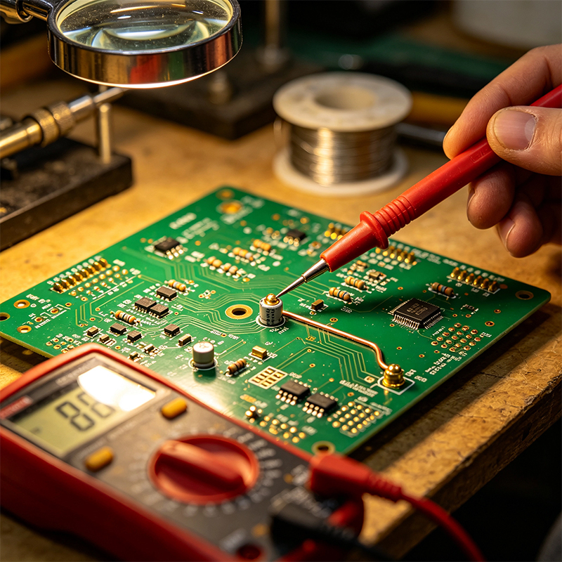
4. Minimize loop area
Every signal trace and its return path form a "loop". The larger the loop area, the more electromagnetic radiation it emits. Good trace design keeps signal and return paths close together, minimizing the loop area.
5. Avoid 90-degree corners
Trace corners should use 45-degree angles or curves, never 90-degree right angles. Right-angle corners cause signal reflections and EMI at high frequencies. When exiting pads, prefer 135° angles.
6. Adjacent layers should route perpendicular
In multi-layer boards, adjacent layers should route in opposite directions — one layer horizontal, the next vertical. This reduces crosstalk between layers.
If your board has high-speed signals (USB, HDMI, DDR memory), traces require even more care.
Impedance Control
High-speed traces must control impedance. Wrong impedance causes signal reflections, distortion, and device failure. Common impedance values are 50Ω single-ended, 90Ω or 100Ω differential.
Impedance depends on trace width, copper thickness, distance to the reference plane, and dielectric constant. All of this must be calculated during design, not discovered during manufacturing.
Differential Pair Routing
USB, PCIe, and HDMI use differential signals — two traces running together, with signals as mirror images of each other. Differential pair routing requires matched lengths (typically within 50 mils), consistent spacing, and symmetrical vias.
Differential impedance is typically 90-100Ω. The two traces should be close and parallel.
Length Matching
Some high-speed signals require multiple traces to be exactly the same length — otherwise, signals arrive at different times, causing timing errors. This is where serpentine routing comes in — routing traces in a snake pattern to add length without increasing straight-line distance.
PCB traces are made through chemical etching. The factory starts with a copper-clad board, coats it with photosensitive material, exposes the trace pattern with UV light, then uses chemicals to dissolve away the unwanted copper. What's left is the traces.
When a trace breaks, the circuit stops working. Common causes:
Too narrow: current overload burns the trace open
Mechanical damage: board flexing or scratching breaks the trace
Manufacturing defects: incomplete etching, misaligned drilling
Corrosion: moisture causes copper traces to oxidize and corrode
PCB traces are the copper lines on a circuit board that conduct electricity — the "nervous system" of the board. When designing traces, you must consider width, spacing, length, corners, and impedance control for high-speed signals. Every single trace is carefully engineered — width, length, direction — all with purpose.
We are a custom manufacturer of flexible PCBs, rigid-flex boards, HDI high-frequency boards, and full PCBA services. Whether your board is a simple 2-layer design or a complex 20+ layer HDI board, we can tailor it to your needs — from design support to PCB fabrication to PCBA assembly, all under one roof. Send us your design requirements, and our engineers will review your trace routing to ensure your board not only works but can be manufactured reliably.

Kaboer manufacturing PCBs since 2009. Professional technology and high-precision Printed Circuit Boards involved in Medical, IOT, UAV, Aviation, Automotive, Aerospace, Industrial Control, Artificial Intelligence, Consumer Electronics etc..


 English



 Wechat
 +86 13670210335
 +86 13670210335
 E-mail