
Date: 2026-07-21
You're designing an electronic product. Maybe a wearable device, an industrial controller, a medical instrument, or an automotive sensor. You've drawn the schematic, selected the components, and received the bare boards. Now what? You need to mount those components onto the boards and turn them into working devices. That process is called PCB assembly.
PCB assembly — also called PCBA — is the process of soldering electronic components onto a bare PCB to create a functional, powered circuit. Simply put, PCB is the empty board; PCBA is the finished product. Turning a bare board into a functional module involves solder paste printing, component placement, reflow soldering, inspection, and testing. If you try to coordinate with multiple suppliers yourself — a board house, component distributors, and an assembly shop — just managing those three relationships can be a nightmare. PCB assembly services bundle all of these steps together so you only need to submit your design files to get finished boards.
In this guide, I'll explain what PCB assembly services are, what they include, how the process works, how quality is controlled, and how to choose the right supplier. Plain English, no fluff.
The global PCB assembly market was valued at approximately $97.88 billion in 2025** and is projected to reach **$103.37 billion in 2026, growing at a CAGR of 6.12%, hitting $148.42 billion by 2032**. Other reports project it to reach **$176.6 billion by 2035.
These numbers tell you one thing: PCB assembly isn't optional — it's essential. As electronics get smaller, denser, and faster, assembly services become more critical and the market keeps growing.
PCB assembly services are not just "soldering boards for you." A complete PCB assembly service typically includes:
1. Component Sourcing
Sourcing all components from your BOM — resistors, capacitors, chips, connectors. Experienced assembly service providers pre-stock common components and only purchase from authorized channels to avoid counterfeit parts.
2. PCB Fabrication
Manufacturing bare boards from your Gerber files. If the assembly service provider has its own PCB fabrication line, boards can go straight to the SMT line — saving shipping and handoff time.
3. SMT Assembly
Using automated pick-and-place machines to solder components onto boards. This is the dominant method, accounting for about 90% of all assemblies. Components sit directly on the board surface — no holes required.
4. Through-Hole Assembly
For components that can't be SMT-mounted (large capacitors, connectors) — wave soldering or hand soldering.
5. Inspection and Testing
AOI (Automated Optical Inspection), X-Ray (for BGA inspection), ICT (In-Circuit Test), FCT (Functional Test) — every board goes through multiple quality checks before shipping.
6. Packaging and Shipping
Passing boards are packaged and shipped to you.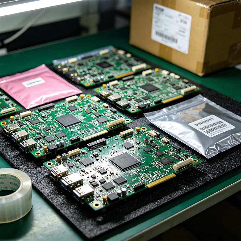
PCB assembly services come in two main models:
Turnkey
You only provide Gerber files, BOM, and Pick & Place data. The supplier handles everything — sourcing components, fabricating bare boards, SMT assembly, through-hole assembly, testing, packaging, and shipping. You do nothing — just wait for the finished boards.
In a turnkey model, the supplier manages the entire PCB production process — from sourcing components and manufacturing bare boards to assembly, testing, and delivery. You work with one manufacturing partner instead of managing multiple vendors for PCB, assembly, tests, and enclosures.
Consignment
You supply all components, and the supplier only does the assembly. This works if you already have a mature supply chain or have already purchased certain components.
Which one to choose? If you're a startup or small team without a dedicated procurement team, turnkey saves you a massive amount of time and effort. If you already have a mature supply chain, or have already purchased certain critical components, consignment might be more suitable.
Turning a bare board into a finished assembly typically involves these steps:
Step 1: File Preparation and DFM Check
The factory receives Gerber files, BOM, and Pick & Place data. A DFM (Design for Manufacturing) check is run first — do component footprints match the pads? Is clearance sufficient? Are fiducials present? This step catches problems before they become expensive physical defects.
Step 2: Solder Paste Printing
A stencil is used to deposit solder paste precisely onto the PCB pads. Solder paste is a mixture of microscopic solder spheres and flux — about the consistency of toothpaste.
Step 3: Component Placement (SMT)
Pick-and-place machines position components onto the pasted pads. High-speed machines handle small passives; high-precision machines handle ICs.
Step 4: Reflow Soldering
The populated board goes through a reflow oven. Heat melts the solder paste, then cools to solidify, permanently attaching the components.
Step 5: Through-Hole Assembly (DIP/THT)
Some components (large capacitors, connectors) can't be placed by SMT machines — they're inserted manually or by machine, then wave-soldered or hand-soldered.
Step 6: Inspection (AOI, X-Ray, ICT, FCT)
After reflow, boards go through Automated Optical Inspection (AOI) . For hidden joints (like BGAs), X-Ray inspection is required. After power-up, ICT (In-Circuit Test) checks component-level connections, and FCT (Functional Test) verifies overall board functionality.
PCB assembly quality is governed by IPC-A-610. It's the most widely used electronics assembly standard in the world, using hundreds of color photos and illustrations to show what good solder joints look like versus bad ones.
IPC-A-610 divides products into three classes:
Class 1 (General Electronic Products) : Function is all that matters — cosmetic imperfections are acceptable. Toys and basic appliances fall here.
Class 2 (Dedicated Service Electronic Products) : Requires continuous, reliable operation — the default standard for most commercial and industrial electronics. Phones, computers, telecom gear.
Class 3 (High-Performance Electronic Products) : Aerospace, medical, defense — the strictest standards.
The companion standard is IPC-J-STD-001 (soldering process requirements). Choosing the right class depends on where your product will be used. Most PCBA projects default to Class 2; medical and aerospace products must use Class 3.
If your product uses flex PCBs or rigid-flex boards, assembly is significantly harder than rigid board assembly.
Flex boards lack rigidity — they warp, shift, and misalign during paste printing and placement. They must be mounted on rigid carriers from paste printing through placement and reflow.
Rigid-flex boards have their own challenge — thermal stress control at the rigid-to-flex transition. The rigid and flex sections expand at different rates during reflow — poor temperature control causes cracking and delamination at the transition.
This is why flex and rigid-flex PCBA requires an experienced manufacturer — a standard SMT shop without flex-specific carriers and optimized reflow profiles will struggle.
We are not a standard rigid-only PCB shop. We are a one-stop manufacturer that designs and makes flexible PCBs, rigid-flex boards, HDI high-frequency boards, and then does full PCBA.
All in-house: PCB fabrication, SMT, DIP, testing, and assembly under one roof. No hand-offs.
Flex/rigid-flex expertise: Dedicated carriers and reflow profiles for flex boards. Hundreds of flex PCBA projects completed.
High-precision placement: Supports 01005 passives, 0.4mm pitch QFN, and BGAs.
SPI + AOI + X-Ray: Every step from paste to final assembly is inspected.
IPC-compliant: Fabrication and inspection to IPC-A-610 and IPC-J-STD-001 — Class 1, 2, and 3.
In-house FCT fixture design: Custom functional test fixtures built for your product.
Free DFM review: Send your Gerber and BOM, get a DFM report within 24 hours with potential issues identified.
Projects we've served: consumer electronics (TWS earbuds, smartwatches), industrial (PLCs, motor drives), automotive (BMS, camera modules), medical (patient monitors, glucometers), communications (routers, optical modules).
Three simple steps:
Send your files: Gerbers, BOM, and Pick & Place data if available.
We review and quote: Within 24 hours, you'll receive a DFM report, sample and volume pricing, and lead time estimate.
Sample, then scale: We build 10-20 samples. You test functionality and reliability. Then we move to pilot and volume production.
PCB assembly is the last mile from a drawing to a real product — and it's the step where the most can go wrong. One bad solder joint on a board with hundreds of components can kill the whole assembly.
If you're looking for a reliable PCB assembly partner, especially if your product involves flex PCBs, rigid-flex boards, or high-density SMT, send us your files. We won't push a contract — we'll first run a free DFM review and let our expertise speak.
When you contact us, please include:
Product type and basic functionality
Whether it uses flex or rigid-flex boards
Estimated annual quantity (samples, small batch, or mass production)
We'll give you an honest answer — what we can do, what we can't, and how to modify your design to make it work.

Kaboer manufacturing PCBs since 2009. Professional technology and high-precision Printed Circuit Boards involved in Medical, IOT, UAV, Aviation, Automotive, Aerospace, Industrial Control, Artificial Intelligence, Consumer Electronics etc..


 English



 Wechat
 +86 13670210335
 +86 13670210335
 E-mail