Date: 2026-01-21
Imagine you’ve just baked a large sheet of cookies. You don’t serve the whole pan—you separate them into perfect, individual pieces. In the world of electronics manufacturing, PCB depaneling is that exact same step, just with circuit boards instead of cookies.
When you look at a circuit board assembly quote, you’re usually not thinking about how it goes from a big panel in the factory to a single board in your hand. But this final step—safely separating the individual boards—is way more important than it sounds. Get it wrong, and you can turn a perfectly good assembly into a pile of damaged or stressed boards.
So, what is it, and why should you care? Let’s break it down.
Simply put, PCB depaneling is the process of separating multiple, smaller printed circuit boards from a larger, connected panel they were manufactured on. This large panel is called a "fabrication panel" or "assembly panel."
Think of this panel as a sheet of postage stamps. All the stamps (your individual PCBs) are printed together on one sheet for efficiency, but they need to be carefully torn apart to be useful.
Manufacturers build boards in panels for one main reason: speed and cost. It’s much faster and cheaper for automated machines to populate, solder, and test one large panel holding 10 small boards than to handle 10 tiny, individual boards. Once all the assembly and testing is done, it's time to sing "Break Free" and separate them.
Not all boards are separated the same way. The method chosen depends on your board's design, material, and how fragile its components are. Here are the main ways factories do it:
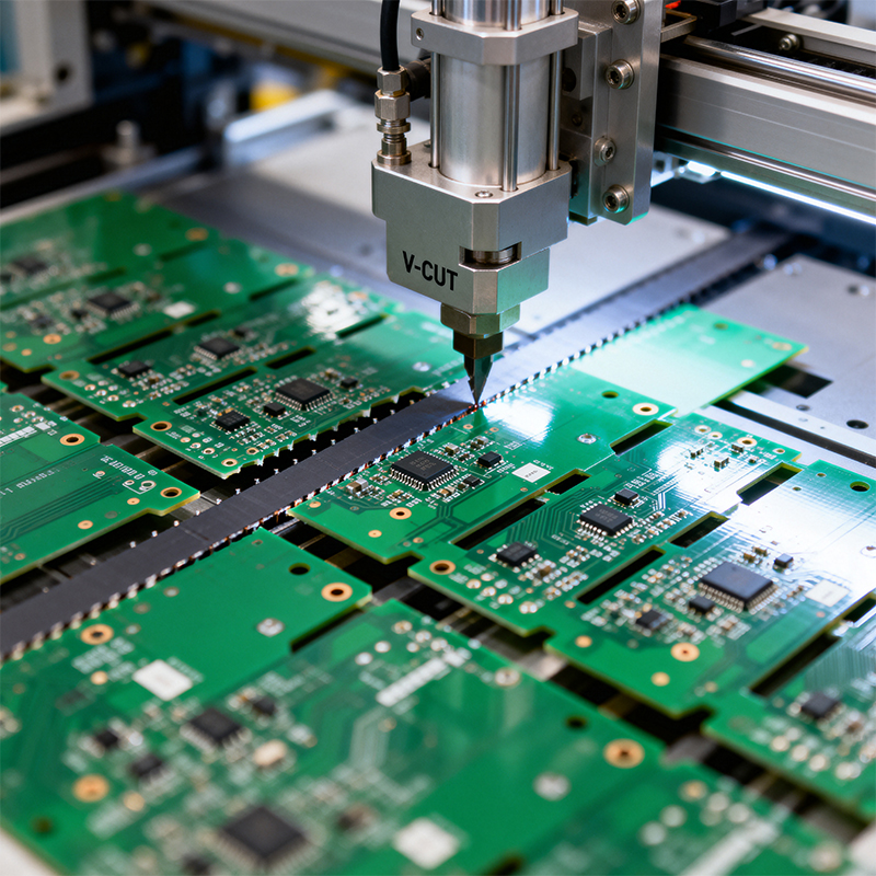
1. V-Scoring (The "Perforated Paper" Method)
How it works: A special blade cuts shallow, V-shaped grooves on the top and bottom of the panel along where the boards need to split.
The analogy: It’s like perforating paper to make it easy to tear. You apply pressure (usually by hand in a fixture or with a simple machine), and the boards snap apart along the scored line.
Pros: Fast, simple, and very low cost. Great for high-volume, simple, rectangular boards.
Cons: The snapping action creates mechanical stress and can leave a rough, slightly jagged edge. Not ideal for ultra-fragile components or boards with components hanging over the edge.
2. Tab Routing with Breakaways (The "Connected Islands" Method)
How it works: Individual boards are held in the panel by small, perforated tabs (like little bridges). A router machine cuts around almost the entire outline of each board, leaving these small connection points. The boards are then manually or mechanically snapped out.
The analogy: Imagine a chocolate bar where each piece is connected by just a tiny bit of chocolate at the corners.
Pros: Leaves a much smoother edge than V-scoring. Allows for non-rectangular board shapes.
Cons: The snapping action still creates some stress. The small "nub" left behind from the tab often needs to be filed down (deburred), adding an extra step.
3. Punching (The "Cookie Cutter" Method)
How it works: A heavy-duty metal die (like a giant cookie cutter) is made in the exact shape of your board. The panel is placed under a press, and the die punches all the boards out at once with tremendous force.
Pros: Extremely fast and consistent for massive, simple board production (think millions of units).
Cons: The initial die is very expensive. The punching force creates huge stress and can only be used on very simple, bare boards with no components near the edges. Rarely used for assembled boards.
4. Routing (The "Precision CNC" Method)
How it works: A high-speed, computer-controlled routing bit (like a tiny, super-fast drill bit) cuts completely through the panel material, following the exact outline of each board. This fully frees the board with no need for snapping.
Pros: Delivers the cleanest, smoothest edges. Produces almost zero mechanical stress or vibration on the components. Works for any board shape.
Cons: Slower and more expensive than V-scoring or tab routing. It's the "premium" method for high-value or sensitive assemblies.
5. Laser Depaneling (The "High-Tech Light Saber" Method)
How it works: A powerful, focused laser beam vaporizes the panel material along the board outlines. No physical contact with the board at all.
Pros: The ultimate in precision and zero mechanical stress. Creates sealed, smooth edges. Perfect for fragile, high-density boards with components very close to the edge.
Cons: The most expensive method due to high equipment costs. Slower than routing for thick panels.
Choosing the wrong method isn't just about rough edges. It can cause real, hidden damage:
Micro-cracks in Solder Joints: The shock and vibration from snapping can create tiny, invisible cracks in the solder joints of components, especially large BGAs. These cracks can cause the board to fail weeks or months later in the field—a nightmare to diagnose.
Component Damage: Ceramic capacitors are brittle. A sharp shock can crack them internally, leading to electrical failure.
Delamination: The force can separate the layers of the PCB itself, especially near the edges.
PCB depaneling isn't an afterthought; it's the last critical step of quality assembly. When you're evaluating a PCBA partner, ask them about their depaneling process. For simple consumer boards, V-scoring might be perfectly fine. But if you're building complex, dense, or high-reliability electronics, you need a partner who understands the risks and invests in the right tools.
At Kaboer, our factory in Shenzhen is equipped with multiple depaneling solutions. We don't just default to the cheapest method. We look at your board's design—the component placement, the board shape, and the reliability requirements—and choose the method (often precision routing) that ensures your boards arrive in your hands as flawless as when they left our assembly line. It’s this attention to the final, often overlooked detail that separates a good assembly house from a true manufacturing partner.
Kaboer manufacturing PCBs since 2009. Professional technology and high-precision Printed Circuit Boards involved in Medical, IOT, UAV, Aviation, Automotive, Aerospace, Industrial Control, Artificial Intelligence, Consumer Electronics etc..