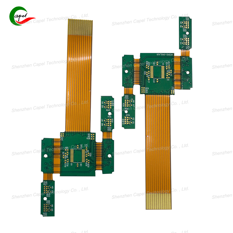
Imagine an engineer spending 8 hours manually redrawing flexible layers for a rigid-flex PCB—only to realize the bend radius is too small, forcing a complete redo. Or wasting 3 days fixing errors because the software didn’t flag a conflict between rigid and flexible components. For rigid-flex board development, these delays aren’t just frustrating—they push projects past deadlines and inflate costs.
The good news? Modern PCB design software (like Altium Designer, Cadence Allegro) has built-in tools to solve these problems. The catch? Most engineers only use 40% of their software’s capabilities. Below are 5 actionable tips to cut design time by 30% and avoid costly mistakes—backed by real engineering workflows.
Rigid-flex PCBs have mixed layers (rigid FR4, flexible polyimide)—and mixing them incorrectly is a top cause of design failures. Instead of drawing layers separately, use your software’s Layer Stack Manager (available in Altium and Cadence) to:
-
Drag-and-drop rigid/flexible layers to match the physical design (e.g., 2 rigid layers on top/bottom, 1 flexible layer in the middle).
-
Auto-calculate the minimum bend radius for flexible layers (critical—too small, and the PCB cracks during use). For example, Altium’s tool flags if the bend radius is less than 3x the flexible layer thickness (a industry standard).
A consumer electronics team in California cut their layer design time from 6 hours to 1 hour using this tip—no more manual checks.
Rigid and flexible areas have different design rules (e.g., component placement: no heavy chips on flexible areas). Manually checking these rules takes hours—but software like Cadence Allegro has Flexible Area Rules to automate the process:
-
Define flexible zones (e.g., a 2cm section of the PCB that bends) and set rules: "No components over 5g in flexible zones" or "Trace width must be ≥0.2mm in flexible areas".
-
The software highlights violations in real time (e.g., a 10g chip placed on a flexible zone) before you finalize the design.
A medical device company in Germany used this to reduce design errors by 60%—they no longer had to rework PCBs because a sensor was placed on a flexible area.

You can’t tell if a rigid-flex PCB bends correctly from a 2D layout. That’s why tools like Altium’s 3D Preview are game-changers:
-
Rotate the 3D model to simulate how the PCB bends (e.g., fold it 180° like a foldable phone).
-
Check for collisions: Does a rigid component scratch the flexible layer when bent? Or does the bend pull on a solder joint?
A drone manufacturer in China used this to fix a critical issue: their 2D design looked fine, but the 3D preview showed the flexible layer would stretch too much during flight—they adjusted the design in 30 minutes, avoiding a prototype failure.
Rigid-flex PCBs need separate BOM entries for rigid and flexible components (e.g., rigid FR4 substrates vs. flexible polyimide). Manually creating this BOM takes 4+ hours—but software like KiCad has Auto-BOM Tools for rigid-flex:
-
Tag components/layers as "rigid" or "flexible" during design.
-
The software generates a BOM that splits parts by type (e.g., "Rigid components: 5 chips, 10 resistors; Flexible components: 2 flexible connectors, 1 polyimide layer").
A automotive electronics team in Texas cut their BOM time from 5 hours to 45 minutes—no more manual sorting of parts.
Rigid-flex board design is complex, but your software doesn’t have to make it harder. By using layer stack managers, flexible area rules, 3D previews, and auto-BOM tools, you can turn days of work into hours—and avoid the mistakes that sink projects.
The best part? These tips work for all major software (Altium, Cadence, KiCad). Start with one tip (e.g., Layer Stack Manager) and see how much time you save—your deadlines (and budget) will thank you.
Founded in 2009, our company has deep roots in the production of various circuit boards. We are dedicated to laying a solid electronic foundation and providing key support for the development of diverse industries.
Whether you are engaged in electronic manufacturing, smart device R&D, or any other field with circuit board needs, feel free to reach out to us via email at sales06@kbefpc.com. We look forward to addressing your inquiries, customizing solutions, and sincerely invite partners from all sectors to consult and collaborate, exploring new possibilities in the industry together.