Date: 2026-01-26
Imagine you have a new circuit design. You need a physical board to test it, and you need it now. The traditional way—sending files to a PCB fab, waiting for shipping—could take days or even weeks. What if you could turn that digital design into a working prototype in your own workshop in a matter of hours?
This is where PCB milling comes in. It's not the standard method for making thousands of boards, but for rapid prototyping, specialized one-offs, or urgent fixes, it's like having a mini circuit board factory on your desk.
To understand milling, think about how standard PCBs are made: the etching process. You start with a board completely covered in copper, and you use chemicals to etch away all the copper you don't want, leaving your circuit traces behind. It's like a bathtub dissolving everything except the protected parts.
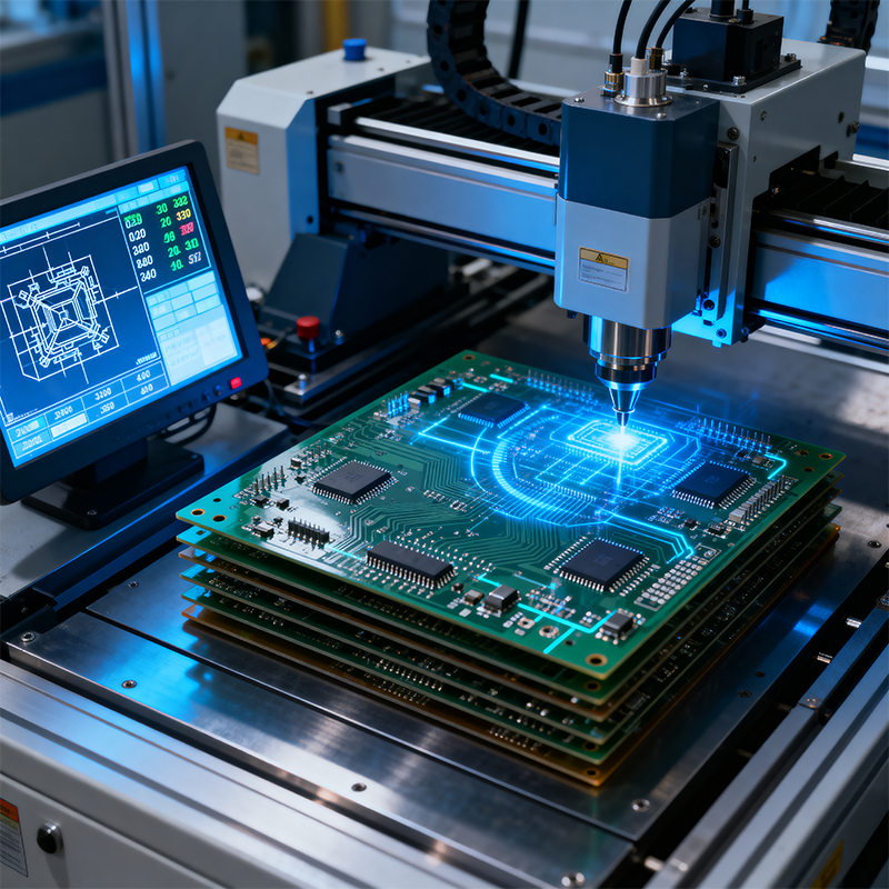
PCB milling flips this idea. Instead of using chemicals, it uses a tiny, spinning drill bit called an end mill. A computer-controlled machine (a CNC mill) drives this bit across a bare copper-clad board. The bit's job is simple: to mechanically cut away or mill off the copper you don't want.
Think of it like a highly precise engraving tool or a miniature router. It's subtractive manufacturing: you start with a solid block of material and remove what isn't part of your final product. The result is your custom circuit, carved directly out of the copper.
Design: You create your PCB layout in any standard design software (like KiCad, Eagle, or Altium).
Preparation: Instead of generating Gerber files for a fab house, you generate toolpaths for your CNC machine. Specialized software (like FlatCam or a machine's own software) translates your traces and outlines into the precise X, Y, and Z movements the milling bit must follow.
Milling: You fix a blank copper-clad board to the machine's bed. The process typically has two main steps:
Isolation Routing: A very fine V-shaped bit traces the outline of all your copper traces. It cuts a tiny channel (an "isolation path") on either side of each trace, separating it from the rest of the copper "sea." This leaves your desired circuit pattern standing proud.
Contour Cutting: A larger bit then cuts the entire outer shape of your PCB from the larger panel, freeing your finished board.
Cleaning & Assembly: You brush off any small copper debris ("swarf"), and your board is ready for you to solder components onto. No chemical cleaning or waiting for a surface finish is required.

Why would you choose this hands-on method?
Speed: This is the biggest draw. From finished design to holding a board can be under an hour. It’s perfect for the "I need to test this today" phase of development.
No Chemicals: There are no toxic etchants (like ferric chloride) to handle, store, or dispose of. It's a clean, office-lab-friendly process.
Iteration is Cheap and Instant: Made a mistake in your design? Fix the file and mill a new version in 30 minutes. This encourages experimentation and rapid learning.
It's Not Just for FR4: You can mill other materials easily, like acrylic for front panels, or even aluminum for enclosures, with the same machine.
PCB milling is a fantastic tool, but it's not a replacement for traditional fabrication.
Limited Resolution: The physical size of the milling bit limits how fine your traces can be and how close they can get. You can't mill the ultra-fine traces and spaces found in a modern smartphone. Typical limits are around 0.2mm (8 mil) trace/space.
No Plated Holes: The mill can drill holes, but it can't chemically plate their insides to connect layers. This makes multi-layer boards very complex. Milling is best for simple single or double-sided boards.
Slower for Quantity: Making one board is fast. Making ten of the same board is ten times slower. It does not scale for production.
Surface Finish: The milled copper is raw and will oxidize. It lacks the nice solderable finish (like ENIG or HASL) of a professionally made board, which can make soldering a bit trickier over time.
Think of PCB milling as the ultimate prototyping and specialty tool. It shines when:
You are in the early R&D or prototyping loop and need instant feedback.
You need a single, highly customized board (like a specific sensor interface) and can't wait.
You are teaching or learning electronics, and the quick, visible process is invaluable.
You need a board made from an unusual material that can't be chemically etched.
PCB milling puts the power of rapid circuit creation directly in the hands of the designer. It bridges the gap between a digital idea and a tangible object faster than any other method. While it won't produce the high-density, complex boards that fill our consumer gadgets, it is an indispensable tool for innovation, education, and solving urgent hardware problems. In the world of electronics development, speed and agility are everything, and the milling machine delivers just that.
Kaboer manufacturing PCBs since 2009. Professional technology and high-precision Printed Circuit Boards involved in Medical, IOT, UAV, Aviation, Automotive, Aerospace, Industrial Control, Artificial Intelligence, Consumer Electronics etc..