Date: 2026-01-14
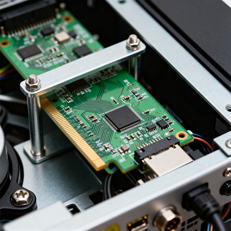
If you open up any electronic device, you'll see various components fixed onto a circuit board—that process is PCB Mount. Simply put, PCB Mount refers to the complete process of accurately installing electronic components onto a printed circuit board (PCB). This term encompasses everything from initial design considerations to actual soldering manufacturing and final quality inspection.
Through-hole technology is "grandfather's era" tech, but it still shines in many applications today. This method requires pre-drilled holes in the PCB. Component leads pass through these holes and are soldered on the opposite side. Think of large electrolytic capacitors, transformers, and connectors—many use this mounting method.
Best for:
Connectors needing to withstand mechanical stress
High-power or high-current components
Test fixtures or frequently replaced parts
Industrial or automotive applications with extreme reliability requirements
The smartphone or laptop you're using right now—about 99% of its components are mounted using SMT. Components are placed directly onto pads on the PCB surface and "stuck" to the board through reflow soldering. This allows for smaller, lighter circuit boards at lower production costs.
Best for:
Almost all consumer electronics
Circuits requiring high-density layouts
High-volume production
Products sensitive to size and weight
Most real-world products actually use mixed mounting—some components through-hole, others surface mount. For example, main controller chips and resistors/capacitors might use SMT, while power connectors and buttons use through-hole. The key lies in properly sequencing these two processes.
Pad size, shape, and spacing directly affect soldering success rates. Pads too small risk weak solder joints; pads too large may cause component shifting. A good rule of thumb: pads should be 20-30% larger than component leads.
Automated production lines need space to operate. For instance, pick-and-place machines need sufficient "keep-out" areas for nozzle movement, while wave soldering requires considering solder flow direction. These production considerations should be part of early design planning.
The placement of high-power components affects overall heat dissipation. Distributing heat-generating components evenly, avoiding hot spots, can significantly improve product lifespan.
Small resistors or capacitors lifting on one end during reflow soldering, standing up like tombstones—usually caused by asymmetric pad design or improper temperature profiling.
Too little solder causing poor contact, or too much solder creating shorts. These seemingly opposite problems often stem from the same root cause: improper pad design or solder paste printing.
Static electricity, mechanical stress, or thermal shock can all damage sensitive components during mounting. BGA chips and QFN packages require extra careful handling.
Considering these factors can help you make smart decisions:
Product Positioning:
Cost-sensitive consumer electronics? Prioritize full SMT
High-reliability industrial equipment? May require mixed technology
Low-volume custom products? Through-hole might offer more flexibility
Production Volume:
High volume: Fully automated SMT lines offer highest efficiency
Low volume: May need to retain manual soldering flexibility
Prototype phase: Both manual soldering and small-batch SMT are options
Technical Complexity:
Simple circuits: Traditional through-hole might be more economical
Complex functionality: SMT is almost always the choice
Special requirements (like flex boards): Need specialized processes
Unless absolutely necessary, choose components with standard footprints. Non-standard packages increase production costs and risks.
How will you test after assembly? Are test points sufficient? These should be considered during design.
The smartest approach is consulting manufacturers before starting your design. They'll tell you which design choices affect mounting quality and cost.
Few products achieve perfect manufacturability in their first version. Leaving room for optimization is wise.
Running our own PCBA factory in Shenzhen over the years, we've seen too many projects delayed due to mounting issues. A few points particularly worth sharing:
The Importance of Material Compatibility:
One customer's design was theoretically perfect, but production revealed that a component's terminal coating wasn't compatible with our standard solder paste, causing numerous cold joints. Now we offer specialized BOM compatibility checking to eliminate such issues during design.
Communicating Design Intent:
Design files and actual intentions sometimes differ. We've developed a habit: for any new design, our engineers first discuss critical component mounting requirements with customers rather than simply following drawings.
Flexible Production Configuration:
Our production lines can quickly switch between full SMT and mixed technology modes. For small to medium batch orders, this flexibility has saved many customers both cost and time.
The Value of Design for Manufacturability:
We provide free DFM checks for customers. The most common suggestions involve optimizing pad designs and component placement. Sometimes a small change can improve yield by over 10%.
Do all your components have available standard footprints?
Does pad design comply with IPC standards?
Have you considered production equipment capability limits?
Are test points sufficient and reasonably located?
Are heat-sensitive components away from high-temperature areas?
Are high-value chips protected against electrostatic discharge?
PCB Mount might seem like just one step in electronics manufacturing, but it bridges design and product, affecting cost, quality, and time-to-market. Whether you choose full SMT, through-hole, or mixed technology, what matters most is understanding the trade-offs behind each choice.
If you're planning a new product or facing mounting challenges, feel free to reach out. We've handled various mounting requirements and might offer some practical advice.
Kaboer manufacturing PCBs since 2009. Professional technology and high-precision Printed Circuit Boards involved in Medical, IOT, UAV, Aviation, Automotive, Aerospace, Industrial Control, Artificial Intelligence, Consumer Electronics etc..