Date: 2026-01-14
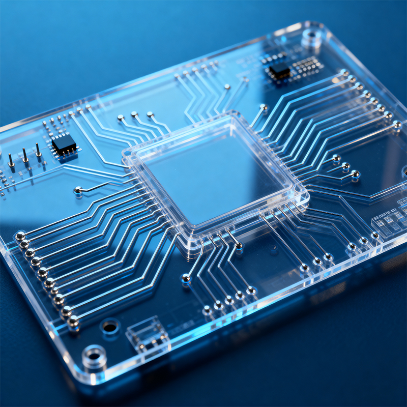
Have you ever imagined a circuit board that’s as see-through as glass? It might sound like a prop from a sci-fi movie, but transparent PCB boards are very much a real technology today. From those eye-catching LED lighting effects to consumer electronics pushing aesthetic boundaries, transparent circuits are quietly expanding what’s possible in product design.
Simply put, a transparent PCB is an alternative to traditional circuit boards that lets you see right through it. But don’t be mistaken—this isn’t about making standard green boards transparent. It’s an entirely different technical approach. Transparent PCBs typically use clear substrate materials (like glass or special plastics) paired with transparent conductive layers to create functional circuits.
The most established transparent conductive material is Indium Tin Oxide (ITO), which you’ve probably already encountered in your smartphone’s touchscreen. When this material is finely patterned onto a transparent substrate, it forms “invisible” circuits capable of carrying electrical signals.
Imagine:
Subtle circuit patterns visible in high-end gaming peripherals
Smart home panels seamlessly blending with decorative elements
Wearable devices where the circuitry becomes part of the design language
In these applications, circuits are no longer “guts” to be hidden but become integral to the product’s aesthetics.
The most natural fit for transparent PCBs is combining with light sources:
LED strips integrated more seamlessly into glass or acrylic structures
“Invisible” circuits for automotive interior lighting
Integrated lighting systems in retail display cases
Because the circuits themselves are transparent, light passes through more evenly, creating unique visual effects.
In some cases, transparency itself is the functional need:
Experimental setups requiring observation or access from both sides
Smart features integrated into shop windows or glass partitions
Medical devices where simultaneous observation and monitoring are needed
The manufacturing process differs significantly from traditional PCBs:
Material Selection Phase:
Substrates: Typically glass or optical-grade plastics (like PET, polycarbonate)
Conductive layers: ITO is the most common, with emerging options like silver nanowires or conductive polymers
Patterning Process:
Unlike etching copper foil, transparent conductive layers are patterned by:
Depositing a full ITO layer on the transparent substrate
Removing unwanted areas using photolithography or laser etching
Or directly printing conductive ink to form circuit patterns
Component Mounting Challenges:
Soldering components onto transparent materials requires special techniques:
Low-temperature solder pastes to avoid warping or damaging the substrate
Special bonding techniques for heat-sensitive bases
Possibly requiring alternative component packaging
Transparent conductive materials generally can’t match copper:
ITO sheet resistance is typically 10-100 ohms/square, while copper foil is well below 1 ohm/square
This makes them unsuitable for high-current applications
High-frequency signal transmission is also limited
Glass substrates are fragile and need extra protection
Plastic substrates may not tolerate high temperatures
Overall structure may be less robust than traditional FR-4
Manufacturing transparent PCBs is usually more expensive:
Higher material costs
More complex production processes
Potentially lower yields
Specialized design and testing methods required
If you’re considering transparent PCBs, start with these questions:
Is transparency truly essential?
Ask yourself: Is this a core functional requirement or an aesthetic bonus? Is the cost increase justified?
What’s the circuit complexity?
Transparent technology suits relatively simple circuits (LED drivers, touch sensors, etc.) better. Complex multilayer motherboards may not be practical.
What’s your production volume?
Small-batch customization might be feasible, but mass production requires careful supply chain evaluation.
What are the environmental requirements?
Transparent materials may be more sensitive to temperature, humidity, or UV exposure.
If fully transparent PCBs are too costly or technically challenging, consider these alternatives:
Partial Transparency Designs:
Use transparent materials only in specific areas
Hybrid designs combining traditional and transparent PCBs
Visual Transparency Effects:
Traditional PCBs with transparent solder mask
Careful layout creating an “appears transparent” aesthetic
Semi-Transparent Solutions:
Frosted or translucent substrates
Selectively exposing certain circuit areas
Advances in materials science are driving transparent electronics forward:
New materials like graphene may offer better transparent conductive properties
Printed electronics enable lower-cost manufacturing
Flexible transparent substrates open possibilities for bendable transparent circuits
Transparent PCBs are no longer just lab curiosities—they’ve found their niche in the market. For products that need to blend functionality with aesthetics seamlessly, transparent circuits offer unique design freedom. However, like any emerging technology, they require designers to understand both their strengths and limitations, finding the right balance between what’s ideal and what’s practical.
Whether you’re envisioning the next generation of consumer electronics or tackling a unique engineering challenge, transparent PCBs deserve a place in your design toolkit—as long as you clearly understand where their capabilities begin and end.
Kaboer manufacturing PCBs since 2009. Professional technology and high-precision Printed Circuit Boards involved in Medical, IOT, UAV, Aviation, Automotive, Aerospace, Industrial Control, Artificial Intelligence, Consumer Electronics etc..