Hold a pair of wireless earbuds or a mini smart sensor—these devices are smaller than a AA battery, yet they need to do it all: play music, track heart rate, connect to Bluetooth, and power a battery. This is the "space paradox" of small-size electronics: users want more functions, but less bulk.
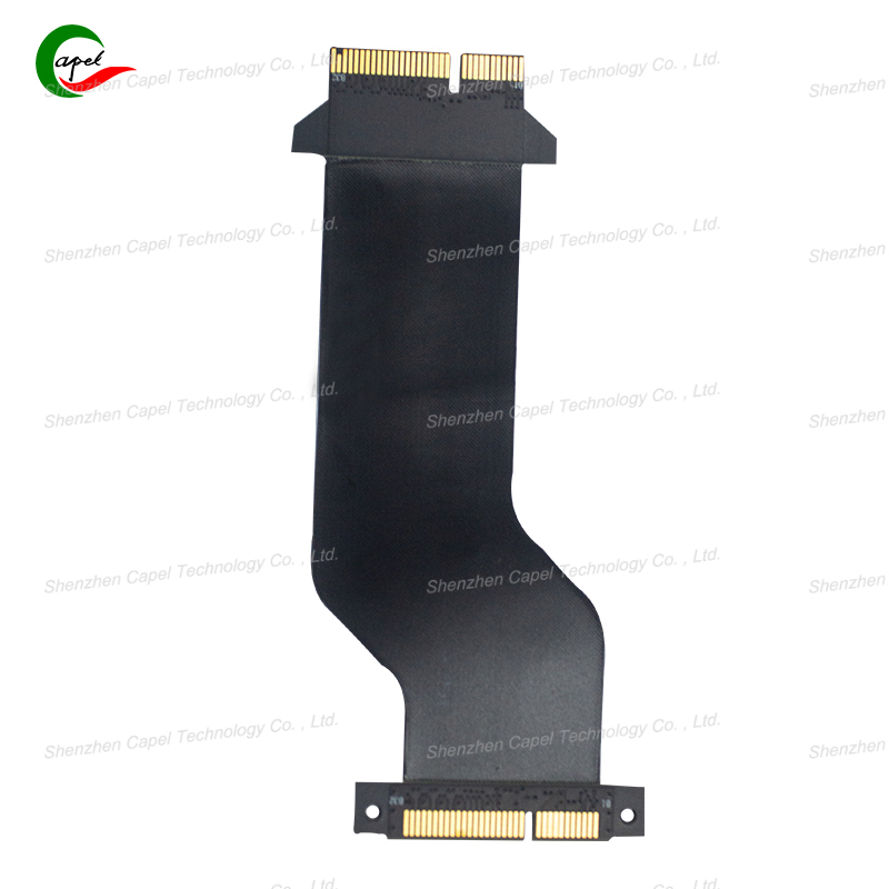
Traditional rigid PCBs are the enemy here. They’re flat, fixed, and take up precious space—you can’t fit a rigid PCB with 5 sensors, a speaker, and a battery into a 1.5cm-wide earbud. But FPCs (Flexible Printed Circuits) change the game. They’re thin, bendable, and can twist around components—turning "impossible" multi-function designs into reality. Let’s break down how FPCs solve the space crisis, with real examples from Apple, 华为 (Huawei), and Fitbit.
Before diving into integration, let’s see why FPCs are better for small spaces:
- Thinness: FPCs are as thin as 0.05mm (thinner than a human hair), vs. 0.8mm for a standard rigid PCB. This means they fit between batteries, screens, and tiny sensors with no extra bulk.
- Flexibility: FPCs bend 180°, fold 360°, or snake through gaps smaller than 1mm—rigid PCBs can’t move at all.
- Single-Board Integration: One FPC can replace 2-3 rigid PCBs (and the messy wires connecting them). A test by the Consumer Technology Association found FPCs reduce a device’s internal space usage by 40% vs. rigid PCBs.
For small electronics, this isn’t just "saving space"—it’s the difference between fitting 3 functions or 8.
Small devices don’t have room for flat PCBs—so FPCs fold into 3D shapes, stacking functions vertically instead of horizontally.
FPCs use "foldable zones" (flexible polyimide) and "rigid zones" (reinforced sections for components). You fold the FPC around the battery or screen, placing sensors on one fold, a chip on another, and a connector on a third—all on one board.
AirPods Pro 2 are just 1.7cm wide, but they include a speaker, microphone, noise-canceling sensor, battery, and Bluetooth chip. Apple uses a single FPC that folds into a "Z-shape":
- Fold 1: Holds the noise-canceling sensor, tucked above the battery.
- Fold 2: Carries the Bluetooth chip, wrapped around the speaker.
- Fold 3: Connects the battery, snaking through a 0.8mm gap.
Without FPC folding, Apple would need 3 separate rigid PCBs—and the earbuds would be 2x thicker.
Small electronics have curved or irregular shapes (e.g., smartwatch bezels, earbud casings). FPCs use "conformal routing"—they follow the device’s contour, instead of forcing a flat PCB into a curved space.
Engineers design FPC traces to match the device’s inner shape: around a curved battery, along a narrow bezel, or even wrapped around a tiny motor. This eliminates "dead space" (gaps where rigid PCBs can’t reach).
The Huawei Watch Fit 2 has a 1.74-inch screen and a slim, curved body—yet it tracks heart rate, blood oxygen, and sleep. Huawei’s FPC uses conformal routing:
- The FPC curves along the watch’s inner bezel, placing the heart rate sensor near the skin (no gap).
- Traces snake around the curved battery, connecting the oxygen sensor to the main chip.
- A tiny "loop" of FPC fits into the watch’s 0.5mm-thick band connector.
A rigid PCB would force the watch to be 30% thicker—ruining its slim design.
FPCs aren’t just single-layer—they use 2-4 flexible layers, each carrying different functions, stacked into one thin board. This is "multi-layer integration": more functions, same tiny footprint.
- Top Layer: Carries signal traces (e.g., Bluetooth, sensor data).
- Middle Layer: Acts as a ground plane (reduces noise, no extra space needed).
- Bottom Layer: Connects power (battery to chip, no separate wires).
All layers are bonded into one FPC, just 0.1mm thick—thinner than a rigid 2-layer PCB (0.4mm).
The Fitbit Luxe is a slim fitness band (just 8.8mm wide) that tracks steps, calories, and stress. Fitbit’s 3-layer FPC packs:
- Top layer: Sensor traces (heart rate, skin temperature).
- Middle layer: Ground plane (keeps sensor signals clear).
- Bottom layer: Power connections (battery to microchip).
A single-layer FPC would need 2x more space to separate power and signal traces—making the band too bulky.
Small devices have no room for bulky components (e.g., resistors, capacitors) mounted on top of PCBs. FPCs use "component embedding": they hide tiny parts inside the FPC layers, not on top.
Engineers etch small pockets in the FPC’s polyimide layers, place tiny components (0.4mm x 0.2mm) inside, then cover them with a thin copper layer. The components are protected, and the FPC stays flat and thin.
The Sony Xperia Ear Duo is a wireless earbud that plays music and lets users hear ambient sound. Sony’s FPC embeds:
- Tiny capacitors inside the FPC layers (no bulky top-mounted parts).
- A 0.3mm resistor hidden under the signal trace (no extra space).
This cuts the FPC’s "height" by 50%—letting the earbuds fit comfortably in small ears.
Small-size electronics don’t have to choose between "small" and "functional"—FPCs let them have both. By folding into 3D shapes, following device contours, stacking layers, and embedding components, FPCs turn tiny spaces into powerhouses of function.
Apple’s AirPods, Huawei’s smartwatches, and Fitbit’s bands all prove this: without FPCs, these devices would be too big, too thick, or too limited. The next time you use a tiny gadget that does it all—remember, the FPC inside is the reason it works.
For engineers designing small electronics, the lesson is clear: stop thinking about flat, rigid PCBs. Start thinking about FPCs—they don’t just fit in small spaces; they redefine what’s possible in them.
Founded in 2009, our company has deep roots in the production of various circuit boards. We are dedicated to laying a solid electronic foundation and providing key support for the development of diverse industries.
Whether you are engaged in electronic manufacturing, smart device R&D, or any other field with circuit board needs, feel free to reach out to us via email at sales06@kbefpc.com. We look forward to addressing your inquiries, customizing solutions, and sincerely invite partners from all sectors to consult and collaborate, exploring new possibilities in the industry together.
