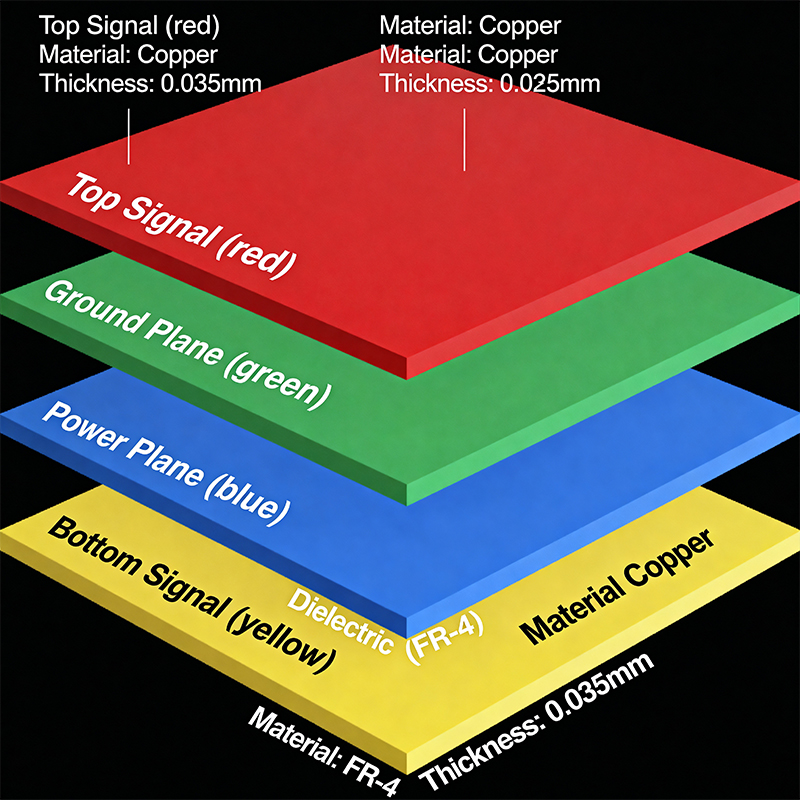
Have you ever struggled with persistent circuit noise on a 2-layer board, barely passed signal integrity tests, or repeatedly failed EMC certifications? If you’re designing a product of medium complexity, moving to a 4-layer PCB might be the smartest and most cost-effective first step you can take. It’s not magic—it’s a classic “best-value” practice in engineering.
1. Core Advantages: What Problems Does It Actually Solve?
Compared to a standard 2-layer board, the heart of a 4-layer structure lies in its two full internal copper layers—typically dedicated as a power plane and a ground plane. This delivers three immediate benefits:
-
A “Highway Home” for Signals: The current of a high-speed signal must form a complete loop. On a 2-layer board, this return path is convoluted and uncontrolled, easily turning into an antenna that radiates noise. The solid ground plane in a 4-layer board provides a direct, low-impedance return path, fundamentally reducing Electromagnetic Interference (EMI).
-
“Quiet and Robust” Power: An independent power plane acts like a large reservoir with very low impedance. It can deliver sudden bursts of current to chips and effectively suppress power supply noise, leading to more stable digital circuit operation.
-
“More Than Doubled” Routing Space: While the layer count only doubles, the effective routing area often more than doubles. Because power and ground traces no longer occupy precious routing channels on the outer layers, engineers can route critical signal traces with much greater ease.
2. The Classic Stackup: Why Has It Dominated for Two Decades?
The most prevalent and reliable 4-layer stackup order in the industry is: Signal (Top) — Ground Plane — Power Plane — Signal (Bottom).
This structure is classic because it strikes the optimal balance between electrical performance and manufacturing cost. The closely adjacent power and ground planes form a natural distributed decoupling capacitor, providing excellent filtering for mid-to-high frequency noise. Meanwhile, critical signal traces can be routed adjacent to the ground plane, achieving the best possible signal integrity.

3. Invisible Pitfalls in Design: Critical Details Beyond Intuition
-
Pitfall #1: Ground Plane Integrity. Avoid cutting slots or splits in the ground plane arbitrarily for routing convenience. A severely fractured ground plane can perform worse than a 2-layer board.
-
Pitfall #2: Stackup Symmetry. Ensure the layer buildup is symmetric about the centerline (e.g., the dielectric thickness from the top layer to the ground plane should equal the thickness from the bottom layer to the power plane). This is key to preventing board warpage during soldering.
-
Pitfall #3: Blindly Chasing High-Spec Materials. For the vast majority of consumer electronics and industrial control products, standard FR-4 material is perfectly sufficient. Unless your signal frequencies exceed 1 GHz or you have special RF requirements, upgrading to premium materials offers minimal performance gain for a significant cost increase.
4. A Practical Checklist for Beginners: How to Start Your First 4-Layer Design
-
Talk to Your Manufacturer First: Before starting layout, request the most proven 4-layer stackup parameters (layer thickness, copper weight, dielectric constant) from your chosen PCB fab. This ensures your impedance calculations match reality.
-
Set Rules Upfront: In your design software, pre-define routing rules (trace width, clearance) for critical nets and prioritize completing the splits for your power and ground planes.
-
Apply the “20H Rule” Flexibly: To further suppress edge radiation, you can inset the power plane from the board edge by about 20 times the distance between the power and ground planes. This is a good practice for sensitive designs.
-
Allow Room for Vias: Place plenty of vias for power and ground nets, especially near IC power pins. This effectively reduces power delivery network impedance.
Conclusion: The Step from “Functional” to “Reliable”
Choosing a 4-layer PCB stackup signifies a transition from being a designer who “solves connectivity problems” to an engineer who “focuses on system performance.” It’s more than just adding two copper layers; it’s an upgrade in design thinking. By following established design conventions and avoiding common pitfalls, you can achieve a massive leap in product reliability, performance, and manufacturability for a minimal cost increase. The next time you face a complex circuit, consider making the 4-layer board your default starting point.