Date: 2025-12-23
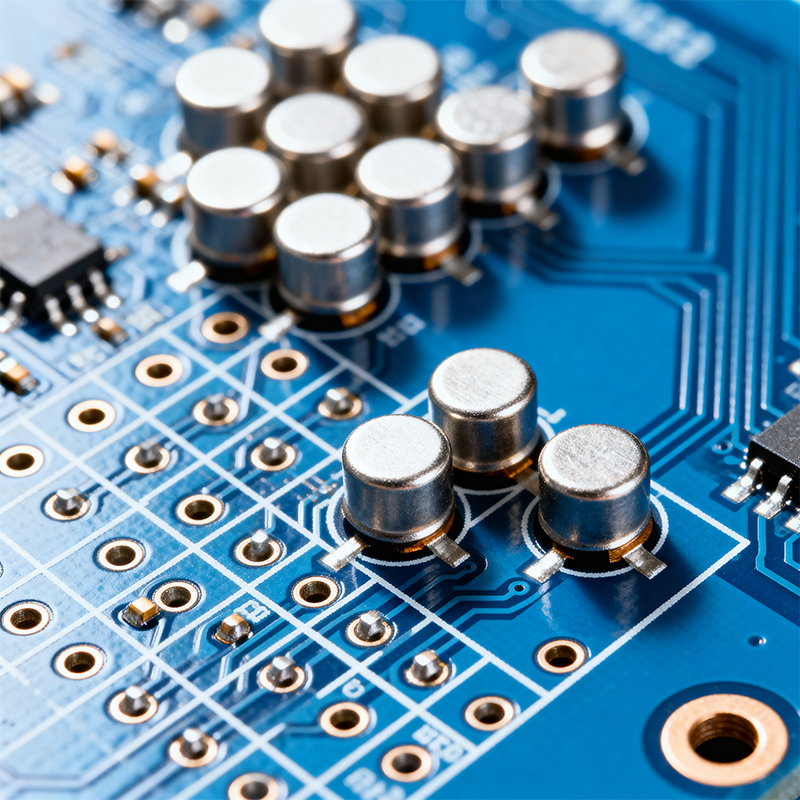
A through-hole printed circuit board (through-hole PCB) is a type of circuit board where electronic components are mounted using leads that are inserted into holes drilled through the board and soldered onto pads on the opposite side. This technology, also known as thru-hole technology (THT), has been a foundational method in electronics assembly since the 1950s and remains vital for specific applications today.
The manufacturing process involves several key steps:
Drilling: Precision holes are drilled through the bare PCB substrate.
Component Insertion: Component leads are inserted through these holes.
Soldering: The assembled board passes through a wave soldering machine, where molten solder creates permanent connections between leads and copper pads.
Cleaning & Inspection: Flux residues are removed, and each connection undergoes quality verification.
While surface mount technology (SMT) dominates modern miniaturized electronics, through-hole PCBs offer distinct advantages:
Through-Hole Advantages:
Mechanical Strength: Components form physical bonds through the board, creating superior mechanical stability
High Reliability: Robust connections withstand mechanical stress, thermal cycling, and high-power applications
Easier Prototyping: Simplified manual assembly and modification processes
Better Thermal Management: Component bodies can dissipate heat directly through the board

Common Applications:
Industrial control systems
Automotive electronics
Power supplies and high-voltage equipment
Military and aerospace electronics
Test and measurement equipment
Connectors and electromechanical components
Hole Size: Must accommodate component leads with appropriate clearance
Pad Design: Annular rings must provide sufficient copper area for reliable solder joints
Component Spacing: Accounts for larger component sizes compared to SMT parts
Thermal Management: Incorporates thermal relief pads to prevent soldering issues
Manufacturability: Considers drill aspect ratios and board thickness limitations
While through-hole PCB usage has declined relative to SMT, it remains indispensable for specific applications. Recent developments include:
Hybrid designs combining through-hole and surface mount components
Advanced automated insertion equipment
Improved solder alloys and fluxes
Specialized applications in harsh environment electronics
Q1: When should I choose through-hole over surface mount technology?
A: Choose through-hole PCBs for applications requiring mechanical robustness, high reliability under stress, high-power components, or easier manual assembly for prototyping and low-volume production.
Q2: Can through-hole and surface mount components coexist on the same PCB?
A: Yes, most modern PCBs utilize mixed technology, with through-hole components for connectors, transformers, and large capacitors, while SMT handles integrated circuits and small passive components.
Q3: What are the main limitations of through-hole PCBs?
A: The primary limitations include lower component density, larger board size requirements, higher drilling costs, and limited compatibility with fully automated assembly lines compared to SMT.
Q4: How does through-hole technology affect PCB manufacturing costs?
A: Through-hole PCBs typically have higher manufacturing costs due to additional drilling operations and often require more manual labor. However, they can reduce total system costs in applications where reliability outweighs miniaturization needs.
Kaboer manufacturing PCBs since 2009. Professional technology and high-precision Printed Circuit Boards involved in Medical, IOT, UAV, Aviation, Automotive, Aerospace, Industrial Control, Artificial Intelligence, Consumer Electronics etc..