
Date: 2026-07-10
You've definitely seen a circuit board before. Green, stiff, covered in copper traces and solder points. But have you ever wondered: what is this board actually made of? Why is it so hard? Why is it green? How do those copper lines get "stuck" onto it?
A circuit board looks simple, but it's actually a composite material sandwich made of multiple layers precisely pressed together. In this guide, I'll break down every material in a circuit board — from the base substrate all the way to the top silkscreen. Plain English, no fluff.
The substrate is the most important part of a circuit board — it's the skeleton. All copper traces and components sit on it. The substrate determines heat resistance, flexibility, and frequency capability.
1. FR4 — The Industry Workhorse
Over 80% of circuit boards use FR4. FR4 stands for "Flame Retardant Level 4" — it's simply woven fiberglass cloth impregnated with epoxy resin pressed into a solid sheet.
Think of it as "fiberglass cloth glued together with resin and pressed into a board." The fiberglass provides strength and rigidity. The epoxy resin bonds the fiberglass layers together and provides insulation and heat resistance.
FR4's glass transition temperature (Tg) is typically 130-140°C, with high-Tg FR4 reaching 170-180°C. Above this temperature, the board starts to soften. FR4's dielectric constant (Dk) is 4.2-4.8, with a dissipation factor (Df) of 0.015-0.020.
FR4 is cheap and "good enough," which makes it the industry standard. Most everyday electronics — appliances, industrial controls, automotive ECUs, IoT devices — all use FR4.
2. Polyimide (PI) — The Soul of Flex Boards
FR4 is rigid — it doesn't bend. Flexible circuit boards use polyimide (PI) film. DuPont has a famous brand called Kapton®. It withstands 260°C, survives hundreds of thousands of bend cycles, and has excellent dielectric properties — the perfect substrate for flexible circuits.
3. Rogers and PTFE — High-Frequency Materials
FR4 struggles above 3-6GHz — signal loss becomes too high. 5G, radar, and satellite communications need low-loss materials. Rogers (ceramic-based or hydrocarbon) and PTFE (polytetrafluoroethylene, Teflon) are the kings of high-frequency. Their dielectric constant can be as low as 2.2-3.5, with loss factors as low as 0.001-0.004. The downside: expensive.
4. Metal-Core — Aluminum and Copper PCBs
LED lighting and power circuits need better heat dissipation. FR4's thermal conductivity is only 0.3-0.4 W/m·K. Aluminum-core PCBs can reach 1-3 W/m·K. Copper-core PCBs are even better — around 400 W/m·K.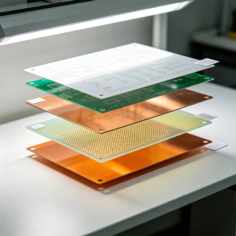
The substrate is the skeleton. Copper foil is the veins — it carries current and signals. Copper foil is thin copper sheet formed by rolling or electroplating, then bonded to the substrate by heat and pressure.
Copper thickness is measured in ounces (oz) . Common thicknesses include 0.5oz (~18μm), 1oz (~35μm), and 2oz (~70μm). 1oz is the most common — there's a well-established relationship between 1oz copper trace width and current capacity. Higher current needs thicker copper.
Two main copper types: electrodeposited (ED) copper and rolled annealed (RA) copper. Rigid boards use ED copper — cheaper and good enough. Flex boards that bend repeatedly must use RA copper — it's more fatigue-resistant.
That green (or red, blue, black) protective layer you see is solder mask, commonly called "green oil." It's a photoimageable polymer coating applied over the copper traces. It does three jobs: prevents copper oxidation, prevents solder bridging, and provides electrical insulation.
Solder mask thickness is typically 10-40 micrometers. Green is the most common — it offers the best visual contrast, the best photo-resolution, and the lowest cost.
Those white letters, symbols, and outlines on the board — "R1," "C2" — are the silkscreen layer. It's made of white epoxy ink printed on top of the solder mask. It's non-conductive and provides information — telling assembly workers where components go and which direction they face.
Copper pads exposed to air oxidize. Oxidized copper doesn't stick to solder. So pads need a surface finish to protect the copper.
The most common surface finishes are:
HASL (Hot Air Solder Leveling) : Cheapest, great solderability, but uneven surface
ENIG (Electroless Nickel Immersion Gold) : Ultra-flat, long shelf life, good for fine-pitch and BGA, but expensive
OSP (Organic Solderability Preservative) : Very cheap, flat, but short shelf life
Immersion Silver / Immersion Tin: Somewhere in between
Substrate preparation: Cut copper-clad laminate to size
Inner layer patterning: Chemical etching creates circuit patterns
Lamination: Stack and press layers under heat and pressure
Drilling: Drill holes and plate with copper
Outer layer patterning: Create outer layer circuits
Solder mask: Apply and expose solder mask to expose pads
Surface finish: Apply HASL, ENIG, or OSP to pads
Silkscreen: Print white text and symbols
Testing: Electrical testing
A circuit board is not one material — it's a combination of materials:
Substrate (FR4 / Polyimide / Rogers / Aluminum): Skeleton — provides strength, insulation, and heat resistance
Copper foil (ED copper / RA copper): Veins — conducts electricity and signals
Solder mask (green oil): Jacket — protects copper traces
Silkscreen (white ink): Labels — provides information
Surface finish (HASL / ENIG / OSP): Protective coating on pads

Kaboer manufacturing PCBs since 2009. Professional technology and high-precision Printed Circuit Boards involved in Medical, IOT, UAV, Aviation, Automotive, Aerospace, Industrial Control, Artificial Intelligence, Consumer Electronics etc..


 English



 Wechat
 +86 13670210335
 +86 13670210335
 E-mail