
Date: 2026-07-06
You've definitely seen a circuit board before. That green board covered in密密麻麻的 silver or gold lines. Some are thin as hair, some a bit wider, snaking their way from chips to resistors to capacitors to connectors. Those thin lines are called PCB traces.
In Spanish, they're called “pistas PCB” — “pista” means “track” or “runway.” It's a perfect name, because traces are exactly that: the “runways” where electrical signals run on a circuit board.
In this guide, I'll explain what PCB traces are, what types exist, and what rules you need to follow when designing them. Plain English, no fluff.
A PCB trace is simply a copper line on a circuit board that conducts electricity. Think of it as the circuit board's version of a wire — except instead of being round and insulated, it's flat copper foil laminated directly onto the board.
Regular wires are round and bulky. PCB traces are flat copper foil “drawn” right onto the board surface — thin and space-saving. They do exactly the same job as wires — carry current and signals from Point A to Point B.
The process of drawing traces in PCB design software is called “routing” — engineers connect components with lines on the computer, just like planning routes on a map.
PCB traces aren't all the same. They come in different types depending on what they carry:
1. Signal Traces
These are the most numerous traces on any board. They carry data signals — whether digital (0s and 1s) or analog (audio, video). Signal traces are usually thin because they don't need to carry large currents.
2. Power Traces
Power traces deliver power from the input to every component. Since they carry current, they're typically much wider than signal traces. If they're too narrow, they'll heat up under load — and in extreme cases, burn open.
3. Ground Traces
Ground traces are the most overlooked but most important traces on a board. They provide a return path for current and also shield against interference and reduce noise. In multi-layer boards, the ground is usually a solid sheet of copper (called a “ground plane”) rather than individual traces.
Beyond these three, there are also differential traces (two traces running together, signals are mirror images of each other to cancel noise), microstrips and striplines (classified by where the trace sits on the board, affecting signal quality), and more.
Traces aren't drawn randomly. Many rules must be followed — or the board might not work, or even burn up.
Rule 1: Width must be sufficient
Trace width determines how much current it can handle. More current = wider trace. Example: on a 1oz copper board, a 0.25mm trace can handle about 1 amp. For higher currents, you need wider traces — or you can open the solder mask and add extra solder on top.
Rule 2: Spacing must be sufficient
Traces can't be too close together. Too close, and you risk leakage, shorts, or signal interference (called “crosstalk”). A good rule of thumb: spacing should be at least as wide as the trace width.
Rule 3: Keep traces as short as possible
The longer a trace, the higher its resistance, the more signal loss, and the more susceptible it is to interference. Engineers aim for: the shortest possible path to make the connection. In practice, there are trade-offs — sometimes you have to go around obstacles.
Rule 4: High-speed signals need impedance control
If your board has high-speed signals (USB, HDMI, DDR memory), the trace impedance must be controlled to a specific value. Wrong impedance causes signal reflections, distortion, and the device may not work. This is why many high-frequency boards require “controlled impedance” — the factory must precisely control trace width, copper thickness, and dielectric thickness to hit the target.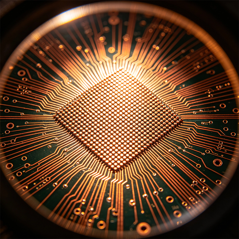
Rule 5: Avoid 90-degree corners
Trace corners should use 45-degree angles or curves, never 90-degree right angles. Right-angle corners cause signal reflections and EMI at high frequencies.
Rule 6: Power and ground come first
Power and ground are the foundation of the circuit. Design them first, then route signals. In multi-layer boards, power and ground are usually solid copper planes (called “power planes” and “ground planes”) rather than individual traces.
PCB traces are made through chemical etching. The factory starts with a copper-clad board, coats it with photosensitive material, exposes the trace pattern with UV light, then uses chemicals to dissolve away the unwanted copper. What's left is the traces.
When a trace breaks, the circuit stops working. Common causes:
Too narrow: current overload burns the trace open
Mechanical damage: board flexing or scratching breaks the trace
Manufacturing defects: incomplete etching, misaligned drilling
Corrosion: moisture causes copper traces to oxidize and corrode
PCB traces are the copper lines on a circuit board that conduct electricity — the circuit board's version of wires.
They come in three main types: signal traces, power traces, and ground traces. Design rules cover width, spacing, impedance, corner angles, and more. Traces are the “nervous system” of the circuit board — without them, components are just disconnected parts that can't work together.

Kaboer manufacturing PCBs since 2009. Professional technology and high-precision Printed Circuit Boards involved in Medical, IOT, UAV, Aviation, Automotive, Aerospace, Industrial Control, Artificial Intelligence, Consumer Electronics etc..


 English



 Wechat
 +86 13670210335
 +86 13670210335
 E-mail