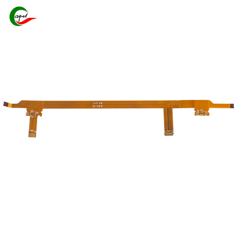
Surface plating is a quiet workhorse in flexible PCB manufacturing, turning fragile copper traces into robust, reliable conductors. It’s not just about looks—this process adds protection, enhances conductivity, and ensures these bendable circuits hold up in tough conditions. Let’s break down the key details.
Flexible PCBs rely on thin copper traces that face unique stress: bending, vibration, and exposure to moisture or chemicals. Plating acts as a shield, preventing corrosion that could break connections. It also strengthens solder joints—critical in devices like foldable phones, where repeated flexing risks loosening components. Without plating, even a small scratch on exposed copper could lead to signal failures.
- Gold Plating: The gold standard for high-reliability uses. Gold resists corrosion and ensures consistent conductivity, making it ideal for medical devices (like pacemakers) or aerospace gear, where failure isn’t an option. It’s often applied as a thin layer over nickel (a "gold over nickel" stack) for extra adhesion.
- Tin or Tin-Lead Plating: A budget-friendly choice for consumer electronics. Tin protects copper from oxidation and works well for solderability—think smartwatches or wireless earbuds. Tin-lead blends (still used in some industrial settings) offer better solder flow but are fading due to environmental regulations.
- Silver Plating: Great for high-frequency applications, like 5G antennas. Silver has superior conductivity to gold but tarnishes more easily, so it’s often sealed with a protective coating. It’s a go-to for radar systems or IoT devices needing fast signal transmission.
Bendability complicates plating. Rigid PCBs sit flat during processing, but flexible substrates can warp or crease, leading to uneven plating. Engineers solve this by using temporary stiffeners during plating or adjusting chemical baths to work with flexible materials like polyimide. Another hurdle: ensuring plating adheres well after thousands of bends. Weak adhesion can cause flaking, especially in automotive sensors that vibrate constantly.
The process starts with cleaning—stripping away oils or oxides from copper traces. Then, a "strike" layer (thin nickel or copper) helps the final plating stick. The PCB is dipped in a chemical bath, where an electric current deposits the metal (gold, tin, etc.) onto the copper. For flexible PCBs, bath temperatures and current levels are fine-tuned to avoid damaging the substrate. Finally, a post-plate rinse removes excess chemicals, ensuring no residue weakens the circuit.
Plating might be invisible to the user, but it’s what makes flexible PCBs tough enough for daily use. From your smartphone to life-saving medical tools, this underappreciated step keeps bendable tech working reliably—no matter how much it’s twisted or tested.
Founded in 2009, our company has deep roots in the production of various circuit boards. We are dedicated to laying a solid electronic foundation and providing key support for the development of diverse industries.
Whether you are engaged in electronic manufacturing, smart device R&D, or any other field with circuit board needs, feel free to reach out to us via email at sales06@kbefpc.com. We look forward to addressing your inquiries, customizing solutions, and sincerely invite partners from all sectors to consult and collaborate, exploring new possibilities in the industry together.
