
Date: 2026-07-15
You've definitely seen an inductor before — copper wire wound around a core, like a little spring. But there's a type of inductor that doesn't use wound wire, doesn't need a core, and is printed directly onto a circuit board, flat like a mosquito coil on the board's surface. That's a printed inductor.
A printed inductor (also called a planar inductor) isn't wound — it's made directly on the PCB using standard circuit board manufacturing processes [0†L20-L23]. Smartphones, RFID tags, power modules, wireless chargers — they all use them [3†L45-L47]. In this guide, I'll explain what a printed inductor is, what it's used for, and how it compares to traditional wire-wound inductors. Plain English, no fluff.
A printed inductor is simply an inductor that's "drawn" directly onto a circuit board.
Traditional inductors are wound — copper wire is wrapped around a core. Printed inductors don't use wound wire. Instead, they use the PCB's copper layers to etch a spiral-shaped trace that acts as the coil [0†L4-L8].
Think of it like a mosquito coil on a circuit board — spiraling around on the surface, creating a magnetic field when current flows through it [4†L4-L8].
Besides single-layer spiral coils, printed inductors can also be multi-layer — spirals on two layers connected by vias to form a "3D" inductor [0†L9-L12]. They can even be made as solenoid types and toroidal types [1†L6-L8].
Here's a quick comparison:
| Feature | Printed Inductor | Wire-Wound Inductor |
|---|---|---|
| How it's made | Etched onto the PCB | Copper wire wound around a core |
| Shape | Flat, like a mosquito coil | 3D, like a spring |
| Height | Very low (<1mm) | Taller (several mm to cm) |
| Integration | Directly integrated on PCB | Separate component, needs soldering |
| Precision | High (etching is precise) | Depends on winding process |
| Cost at scale | Low | Higher |
| Q factor | Moderate | High |
| Power handling | Good for low power | Good for high power |
Wire-wound inductors have higher Q factors, handle more current, and offer larger inductance values [2†L24-L28]. Printed inductors are thinner, flatter, more integrated, and cheaper to produce in volume [2†L18-L21]. No manual winding — the coil is already on the board [0†L38-L43].
The most common printed inductor shape is spiral — circling around on the board [0†L45-L47]. But spirals come in several variations: square, hexagonal, octagonal, and circular [0†L45-L49]. Different shapes have different Q factors and inductance values — circular has the lowest loss, square is the most space-efficient [1†L45-L47].
Printed inductors can be made on a single layer (single-layer spiral) or on multiple layers (multi-layer spiral), with layers connected by vias [0†L50-L54]. Multi-layer designs give you more inductance in the same area, but they also add parasitic capacitance [0†L52-L54].
Beyond spirals, printed inductors can also be made as solenoid types and toroidal types [1†L6-L8]. Solenoid types have a magnetic field distribution closer to traditional inductors; toroidal types have closed magnetic paths and less EMI [1†L33-L35].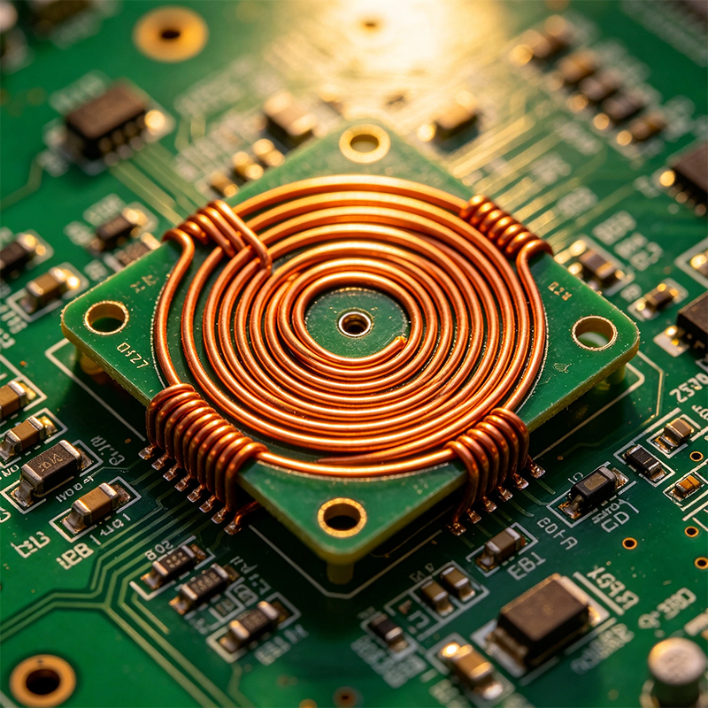
Printed inductors are far more common than you might think:
RFID Tags and NFC: Printed inductors are built directly into the tag's antenna — serving as both inductor and antenna [0†L20-L23].
Smartphones and Wearables: Space is tight inside phones and watches — the flat shape of printed inductors is perfect [5†L36-L40].
DC-DC Power Converters: In low-power modules, printed inductors can be integrated directly onto the PCB [5†L8-L13].
5G and RF Circuits: In high-frequency matching networks, printed inductors' small size and low parasitics are a big advantage [3†L45-L47].
Wireless Charging: The receiver coil is essentially a printed inductor [3†L45-L47].
Flexible Electronics: Printed inductors can be made on flexible substrates like polyimide (PI) — perfect for wearables and flexible circuits [5†L9-L13][5†L45-L48].
Printed inductors aren't perfect. They have a few clear drawbacks:
Lower inductance values: Limited by PCB area, printed inductors usually have lower inductance than wire-wound ones [2†L47-L50].
Lower Q factor: Q factor is generally lower than wire-wound inductors [2†L47-L50].
Limited current capacity: Copper foil thickness limits current handling compared to thick wire [2†L24-L28].
That said, technology is improving these limitations. Printing inductors on flexible substrates [5†L9-L13] and using 3D printing to create 3D structures [3†L4-L9] — printed inductors are capable of more and more.
A printed inductor is a flat coil that's "printed" directly onto a circuit board using standard PCB manufacturing processes.
It doesn't use wound wire or a core — it spirals on the board's surface like a mosquito coil. It's flatter, thinner, and easier to integrate than traditional wire-wound inductors, but inductance and Q factor are usually lower. Common shapes include square, circular, hexagonal, and octagonal [0†L45-L49], with single-layer and multi-layer designs [0†L50-L54].

Kaboer manufacturing PCBs since 2009. Professional technology and high-precision Printed Circuit Boards involved in Medical, IOT, UAV, Aviation, Automotive, Aerospace, Industrial Control, Artificial Intelligence, Consumer Electronics etc..


 English



 Wechat
 +86 13670210335
 +86 13670210335
 E-mail