
Date: 2026-07-15
You've definitely seen it. A factory panel with a grid of identical boards, arranged like a chocolate bar. The boards are connected by thin lines or tiny holes, ready to snap apart. This process of arranging multiple small boards into a single large panel is called PCB panelization.
PCB panelization is simply the practice of designing multiple PCBs on a single larger panel for simultaneous fabrication and assembly. It doesn't sound complicated — but it has a real impact on cost reduction, production efficiency, and manufacturing quality. In this guide, I'll explain what PCB panelization is, why it matters, what methods exist, and what to watch out for in your design. Plain English, no fluff.
PCB panelization is the process of arranging multiple individual PCBs (also called "panels" or "sub-boards") into a single larger panel for simultaneous manufacturing and assembly.
In simple terms, you group small boards together, manufacture and assemble them as one, and separate them afterward.
Why do this? Because PCB fabrication and SMT assembly cost time and money per panel, not per board. Processing one large panel costs about the same as processing one small board — but the large panel can hold dozens of small boards. Panelization turns "one board at a time" into "dozens of boards at a time" — efficiency multiplied.
1. Improves production efficiency
SMT placement machines are high-speed machines — they take roughly the same time to place components on a board, regardless of size. Processing one small board at a time wastes the machine's capability. Panelizing small boards into a large panel lets the machine process dozens of boards in one run, drastically improving efficiency.
2. Reduces production costs
PCB fabrication is charged per panel. One large panel doesn't cost many times more than one small board. By panelizing, the per-board cost of fabrication and assembly drops significantly.
3. Enables automated production
Boards that are too small won't stay on the SMT line — the conveyor can't grip them and the nozzle can't hold them. Panelizing creates a panel large enough for stable handling on the line.
4. Improves handling for manual soldering and rework
For boards with large components or manual soldering, a very small board is hard to hold steady. Panelizing gives operators more handling space, better stability, and higher soldering quality.
There are three main ways to panelize boards: V-cut (V-groove), mouse bites (breakaway tabs), and tab routing.
1. V-cut (V-groove)
V-cut is a V-shaped groove cut into both sides of the board. It snaps apart along the groove. V-cut only works for straight lines — all edges must align on a continuous line. The advantages: easy separation, clean edges, low cost. The limitation: straight lines only — can't panelize irregularly shaped boards.
V-cut depth and angle are critical — typically one-third of the board thickness. Too shallow, and boards won't snap apart. Too deep, and you risk damaging inner layer traces.
2. Mouse Bites (Breakaway Tabs)
Mouse bites are a series of small holes drilled along the board edge, like the perforations on a postage stamp. When you snap the boards apart, the holes break cleanly. Mouse bites work for irregular shapes — round, oval, or curved boards.
The advantage: shape flexibility. The downside: rough edges after separation.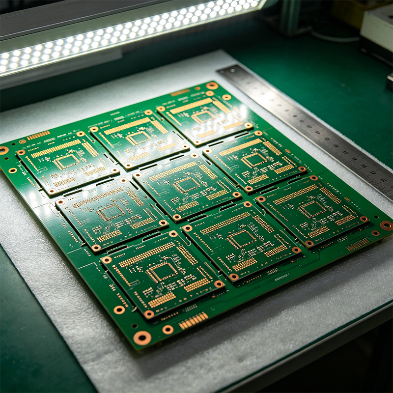
3. Tab Routing
Tab routing leaves small, uncut sections of copper and substrate ("tabs") between boards, while routing away the rest. Tab routing is used for high-precision applications — smooth edges, minimal stress on traces.
Panelization might seem simple, but bad design causes real problems. Here are the core rules:
1. Tooling Strip (Edge Rail)
The panel must have 5-10mm of tooling strip on both sides. The tooling strip gives the SMT line a "handle" — for gripping and conveying. No components should be placed here — only fiducial marks.
2. Fiducial Marks
The panel needs at least 3 fiducial marks — placed at three corners, diagonally positioned — for the pick-and-place machine to locate the board.
3. Panel-to-Board Spacing
Boards need enough spacing between them — V-cut needs 1-2mm, mouse bites need 2-3mm. Too little spacing, and snapping boards apart damages adjacent edges.
4. No Components on the Break Line
All components must stay away from the break lines between boards. Components on the break line will tear during separation.
5. Panel Count
The number of boards per panel depends on final product size and PCB material properties. More isn't always better — too few panels wastes efficiency, too many makes the panel too large for SMT handling.
PCB panelization is covered by industry standards. IPC-2221B, Section 5.3, states that panelization must not introduce residual stress that could affect PCB reliability. IPC-1751A, Section 2.1, requires panel data to be complete and clear, ensuring accurate interpretation by manufacturers.
Using V-cut on non-straight edges: V-cut only works for straight lines — used on irregular shapes, boards won't separate cleanly.
Mouse bites placed near critical traces: Snapping can tear adjacent traces or pads.
Components over the break line: Components will be ripped during separation.
Tooling strips too narrow: The conveyor can't grip the panel.
Fiducial marks incorrectly placed: The pick-and-place machine can't locate the board.
PCB panelization is the process of arranging multiple small boards into a single panel for simultaneous manufacturing and assembly.
It improves production efficiency, reduces per-board cost, and enables automation. There are three main methods: V-cut, mouse bites, and tab routing. Good design requires tooling strips, fiducial marks, adequate spacing, and components kept clear of break lines.

Kaboer manufacturing PCBs since 2009. Professional technology and high-precision Printed Circuit Boards involved in Medical, IOT, UAV, Aviation, Automotive, Aerospace, Industrial Control, Artificial Intelligence, Consumer Electronics etc..


 English



 Wechat
 +86 13670210335
 +86 13670210335
 E-mail