
Date: 2026-07-30
You've definitely seen the dense traces and components on a circuit board. But there's a type of integrated circuit where the "traces" are hundreds of times thinner than a human hair — not soldered on, but "grown" layer by layer using vacuum deposition. That's a thin-film integrated circuit.
In this guide, I'll explain what a thin-film integrated circuit is, how it's made, how it differs from regular chips, and where it's used. Plain English, no fluff.
First, let's get one thing straight: how thin is "thin film"?
Thinner than you can imagine. The components and interconnects in a thin-film IC are typically less than 1 micrometer (μm) thick. One micrometer is 0.001 millimeters. A human hair is about 75 micrometers thick — a thin film is less than one-seventieth the thickness of a hair. The film is deposited on substrates like sapphire, quartz glass, or ceramic using evaporation and sputtering.
Think of it as "drawing circuits on a glass plate with a vacuum coater." On a regular PCB, copper traces are laminated on. On a thin-film IC, the traces are "grown" in place. Line width precision can reach 10 micrometers.
The manufacturing process for thin-film ICs is completely different from regular PCBs. Instead of etching copper foil, it uses several specialized deposition techniques:
1. Vacuum Evaporation
Metal is heated until it vaporizes in a vacuum, and the vapor condenses on the substrate to form a thin film. It's like steam condensing on a lid — except the "steam" is metal and the "lid" is the substrate.
2. Sputtering
High-energy particles bombard a metal target, knocking atoms loose to deposit on the substrate.
3. Chemical Vapor Deposition (CVD)
Gases are introduced into a reaction chamber where they react on the substrate surface to form a solid film.
After deposition, photolithography and electroplating are used to "carve" the film into resistors, capacitors, inductors, and microstrip lines. The finished product is a complete miniature electronic device.
Thin-film ICs are divided into two types based on operating frequency:
Lumped-parameter type: Suitable from low frequencies to microwave bands. Components are relatively larger, good for general RF applications.
Distributed-parameter type: Designed specifically for microwave frequencies. The components themselves are part of the transmission line — ideal for 5G, radar, and other ultra-high-frequency applications.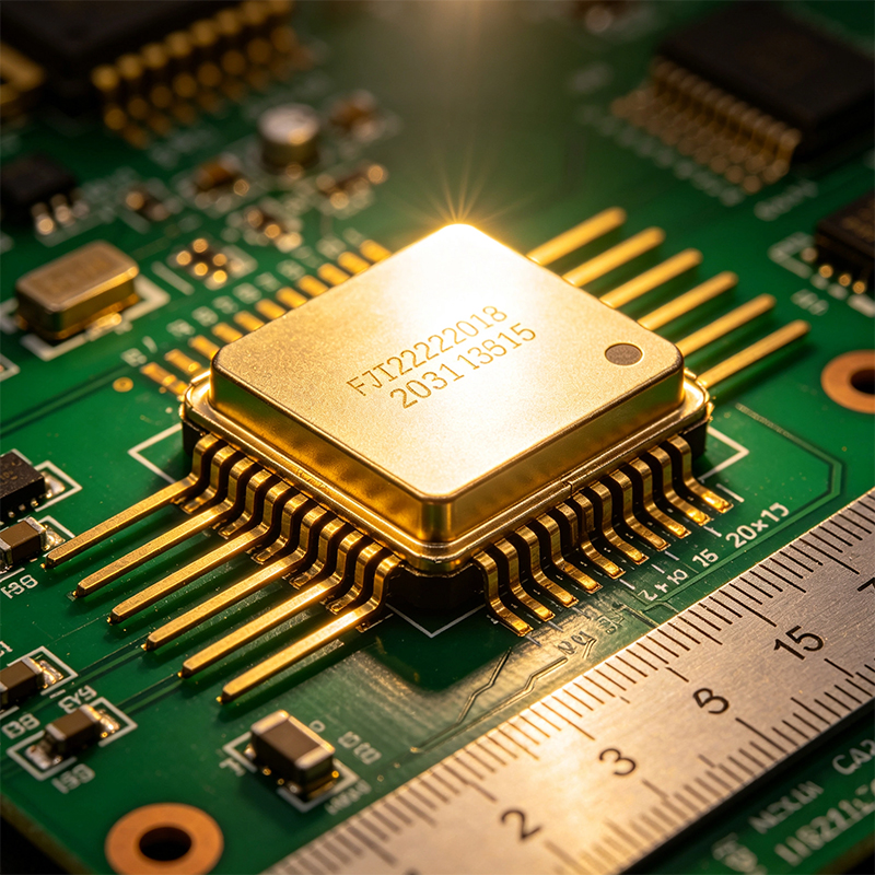
"Thin film" and "thick film" are often compared. The differences come down to two things:
Film thickness: Thin film is less than 10μm, mostly under 1μm. Thick film is over 10μm, typically over 15μm.
Process: Thin film uses vacuum evaporation, sputtering, CVD — precision processes. Thick film uses screen printing — like printing a T-shirt.
| Feature | Thin-Film IC | Thick-Film IC |
|---|---|---|
| Film thickness | <10μm (mostly <1μm) | >10μm (usually >15μm) |
| Process | Vacuum evaporation, sputtering, CVD | Screen printing |
| Precision | Extremely high (±0.01%) | Moderate |
| High-frequency performance | Excellent (up to millimeter-wave) | Moderate (<4GHz) |
| Integration density | High, small size | Lower |
| Cost | High | Low |
| Best for | High-frequency, precision, high-reliability | Small-batch, high-power |
Thin-film precision can reach ±0.01%. Thick film, while less precise, handles higher power and current, and is better for small-batch production. Thin film is for high-frequency precision; thick film is for power and cost-sensitive applications.
Thin-film IC applications are almost always places where regular PCBs can't handle the job:
5G and Microwave Communications: 5G base stations and RF modules need extremely high frequencies and low loss — thin-film is the only choice.
Aerospace: Satellites, airborne radar T/R modules. High reliability, radiation resistance, high temperature tolerance — thin-film has it all.
High-Precision Analog Circuits: Amplifiers, filters, and other circuits demanding extreme precision.
Automotive Electronics: Automotive radar, ADAS (Advanced Driver-Assistance Systems).
Military and High-End Equipment: Thin-film ICs dominate military applications.
Simply put: wherever regular boards can't handle high frequency, high precision, or high reliability — that's where thin-film ICs shine.
A thin-film integrated circuit is a miniature circuit "grown" on a substrate using vacuum evaporation, sputtering, and CVD — with film thickness under 1μm.
The biggest difference from regular PCBs: it's not laminated on, it's grown in place. Extremely high precision, excellent high-frequency performance, and exceptional reliability — but at a higher cost. It's used where "regular boards can't handle it" — 5G base stations, satellite radar, high-end automotive electronics.

Kaboer manufacturing PCBs since 2009. Professional technology and high-precision Printed Circuit Boards involved in Medical, IOT, UAV, Aviation, Automotive, Aerospace, Industrial Control, Artificial Intelligence, Consumer Electronics etc..


 English



 Wechat
 +86 13670210335
 +86 13670210335
 E-mail