
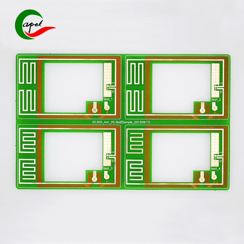


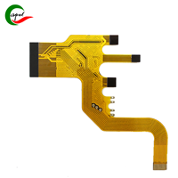
Consumer Card Reader FPC
A short introduction:
Type: Consumer Card Reader FPC
Minimum Line Width/Line Spacing: 0.3mm/0.2mm
Number of Layers: 2 Layers
Thickness: 0.1mm
Surface Finish: Immersion Gold 1 micro inch
Kaboer's Service:
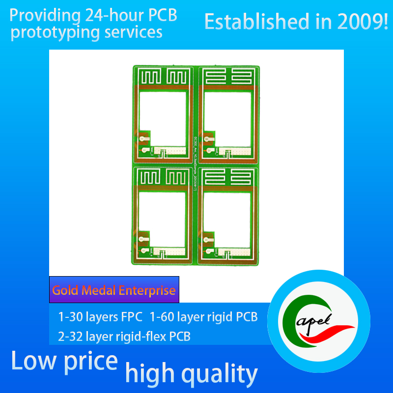
Support Customized 1-30 Layer FPC Flexible PCB, 2-32 Layer Rigid-Flexible PCB, 1-60 Layer Rigid PCB, Reliable Fast Turnaround PCB Prototyping, Rapid SMT PCB Assembly
Industries We Serve:
Medical Device, IoT, TUT, UAV, Aviation, Automotive, Telecom, Consumer Electronics, Military, Aerospace, Industrial Controls, Artificial Intelligence, Electric Vehicles, etc. ......
If you have related needs, please feel free to click the button below to send us an email.
Type: Flexible Circuit Boards (FPC) for consumer card readers, designed for portable card reader devices, with excellent flexible adaptation and signal transmission performance. Whether it is an external SD card reader for cell phones, a built-in memory card interface for notebook computers, or the card slot connection circuit of an all-in-one card reader, it can flexibly adapt to the compact space layout of the card reader (such as the edge of the card slot of a thin and lightweight body, or the curved part of a folding card reader), realizing high-speed data conduction between the memory card and the main control chip, and providing the user with a "Plug and Play, High-speed Transmission The card reader can realize high-speed data conduction between the memory card and the main control chip, providing users with “plug and read, high-speed transmission” experience.
Minimum Line Width / Line Spacing: Reach the high precision standard of 0.3mm/0.2mm. This parameter is optimized for the data transmission characteristics of the card reader: 0.3mm line width ensures that high-speed data signals (e.g., 5Gbps transmission rate of the USB 3.0 protocol) have lower transmission loss (signal attenuation rate of ≤0.5dB/m), reducing the delay in data transmission; 0.2mm line spacing enables multi-channel independent wiring within the limited space of the wiring to support the separation of the power supply, data, and ground lines (e.g., 9-pin parallel signal transmission for SD cards). The 0.2mm wire spacing enables independent multi-channel wiring within the limited wiring space, supports separate transmission of power, data and ground lines (such as 9-pin parallel transmission of SD card signals), avoids signal crosstalk-induced data errors (transmission BER ≤ 10-⁹), and guarantees file read/write integrity.
Layers: 2-layer structure design, through scientific layering to achieve precise division of functions:
signal layer: differential alignment design, optimize the data transmission path, adapted to the high bandwidth requirements of the card reader (support USB 3.0, UHS-I and other high-speed protocols), to ensure that the transmission of large files (eg, 4K video) is smooth and free of lag;
ground layer: a large area of copper foil covering the formation of electromagnetic shielding barriers, effectively isolating the equipment from interference with the internal RF module, power supply, and reducing the data read/write integrity. Ground layer: a large area of copper foil covers to form an electromagnetic shielding barrier, effectively isolating the interference of RF module and power supply inside the device, reducing noise interference in data transmission (signal-to-noise ratio ≥ 60dB), especially suitable for close contact with cell phones, tablet PCs and other strong electromagnetic environment.
Two-layer synergy in the protection of high-speed transmission at the same time, significantly improve the anti-jamming ability to adapt to the complex electromagnetic environment of consumer electronics.
Thickness: The ultimate thinness of only 0.1mm is perfectly suited to the “thin and light” design trend of consumer card readers (e.g., body thickness <5mm). In portable card readers, it can significantly reduce the occupation of the row of wires on the thickness of the device, to release space for the larger capacity of the battery, more card slot layout; in the folding card reader, it can enhance the flexibility of bending (support the minimum bending radius R = 0.5mm), to adapt to the use of frequent opening and closing scenarios, to avoid fatigue breakage of the row of wires.
Surface treatment: the use of immersed gold 1 micro-inch process (nickel layer thickness ≥ 3μm, gold layer thickness ≥ 0.025μm), to bring multiple consumer-grade advantages:
excellent conductivity of the gold layer, reducing data signal transmission loss, to ensure that the contact resistance of the reader interface ≤ 10mΩ, to enhance the stability of data transmission;
immersed gold plating to enhance the abrasion resistance, and can be subjected to frequent insertion and removal of the friction (insertion and removal of ≥ 10000 times), to avoid the oxidation of the contacts after long-term use, to avoid the oxidization of the contacts. Avoiding “card reading failure, data interruption” and other problems caused by contact oxidation after long-term use;
to enhance the reliability of the solder joints, to ensure that the row of wires and the main control chip, the card slot interface of the welded parts of the high and low-temperature environment (-20 ℃ ~ +70 ℃) in contact with the stability of the user's daily use of the environment temperature difference changes.
Kaboer Flexible PCB & Rigid-Flex PCB Process Capability
| Category | Process Capability | Category | Process Capability |
| Production Type |
Single layer FPC / Double layers FPC Multi-layer FPC / Aluminum PCBs Rigid-Flex PCB |
Layers Number |
1-30 layers FPC 2-32 layers Rigid-FlexPCB 1-60 layers Rigid PCB HDI Boards |
| Max Manufacture Size |
Single layer FPC 4000mm Double layers FPC 1200mm Multi-layers FPC 750mm Rigid-Flex PCB 750mm |
Insulating Layer Thickness |
27.5um /37.5/ 50um /65/ 75um / 100um / 125um / 150um |
| Board Thickness |
FPC 0.06mm - 0.4mm Rigid-Flex PCB 0.25 - 6.0mm |
Tolerance of PTH Size |
±0.075mm |
| Surface Finish |
Immersion Gold/Immersion Silver/Gold Plating/Tin Plating/OSP |
Stiffener | FR4 / PI / PET / SUS / PSA/Alu |
| Semicircle Orifice Size | Min 0.4mm | Min Line Space/ width | 0.045mm/0.045mm |
| Thickness Tolerance | ±0.03mm | Impedance | 50Ω-120Ω |
| Copper Foil Thickness | 9um/12um / 18um / 35um / 70um/100um |
Impedance Controlled Tolerance |
±10% |
|
Tolerance of NPTH Size |
±0.05mm | The Min Flush Width | 0.80mm |
| Min Via Hole | 0.1mm |
Implement Standard |
GB / IPC-650 / IPC-6012 / IPC-6013II / IPC-6013III |


![]()
Kaboer manufacturing PCBs since 2009. Professional technology and high-precision Printed Circuit Boards involved in Medical, IOT, UAV, Aviation, Automotive, Aerospace, Industrial Control, Artificial Intelligence, Consumer Electronics etc..


 English
 Automotive Double-Sided Flexible PCB
 Medical Device Double-Sided Flexible PCB
 Medical Device Double-Sided Flexible PCB
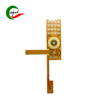 Medical Device Double-Sided Flexible PCB
 Medical Device Double-Sided Flexible PCB
 Double-sided Flexible PCB for Display


 Wechat
 +86 13670210335
 +86 13670210335
 E-mail