
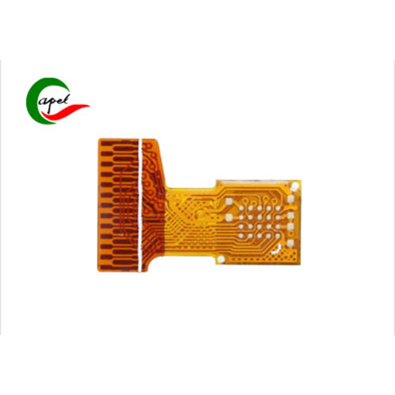

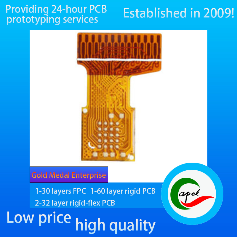

Cell Phone Camera FPC
A short introduction:
Type: Cell Phone Camera FPC
Minimum Line Width/Line Spacing: 0.1mm/0.08mm
Number of Layers: 2 Layers
Thickness: 0.12mm
Surface Finish: Immersion Gold
Kaboer's Services:
Support Customized 1-30 Layer FPC Flexible PCB, 2-32 Layers Rigid-Flexible Circuit Boards, 1-60 Layers Rigid PCB, Reliable Quick Turnaround PCB prototyping,... Rapid SMT PCB Assembly
Industries We Serve:
Medical Device, IoT, TUT, UAV, Aerospace, Automotive, Telecom, Consumer Electronics, Military, Aerospace, Industrial Controls, Artificial Intelligence, Electric Vehicles, etc. ......
If you have related needs, please feel free to send us an email by clicking the button below.
Type: Flexible Printed Circuit (FPC) for cell phone camera, designed for front/rear camera module, with excellent flexible bending performance. Whether it is the built-in main camera with ultra-thin body, the telephoto lens supporting optical image stabilization (OIS), or the image system with multi-camera combination, the FPCs can flexibly adapt to the complex spatial layout inside the cell phone (e.g., the edges of the lens module, the bending transition area between the motherboard and the camera) to realize the precise transmission of image signals, and provide stable circuitry to support the functions of high-definition photography, 4K video recording, and night scene mode.
Minimum line width/line spacing: 0.1mm/0.08mm high precision standard. This parameter is optimized for the high-frequency image signal characteristics of cell phone cameras: 0.1mm line width ensures high-speed transmission of high-definition image data (e.g., 100 megapixel photos, 8K video), while 0.08mm line spacing realizes dense wiring within the limited space of the wiring and supports parallel transmission of multi-channel signals (e.g., independent transmission of signals from the main camera and the depth-of-field lens), which reduces imaging delays due to signal congestion and ensures clear details and no shading on the screen. Details are clear and free of ghosting.
Layers: 2-layer structure design, through scientific layering to achieve fine signal management:
Signal layer: Differential routing design to optimize the transmission path of image data and focus control commands, to adapt to the camera's high-bandwidth signal requirements (such as tens of gigabytes of image data transmission per second);
Ground layer: Large-area copper foil cover, forming a stable electromagnetic shielding barrier, effectively isolating the phone's internal RF, battery and other components from interference, ensuring the purity of the image signal. Interference, to ensure the purity of the image signal, reduce imaging noise.
Two-layer synergy significantly reduces the risk of signal crosstalk, especially suitable for high-end cell phone camera scenes that support “HD imaging + real-time preview” dual-function.
Thickness: only 0.12mm of the ultimate thin and light characteristics, perfectly suited to the smartphone “thin” design trend (such as body thickness <8mm). In the structure of the cell phone's internal space, it can significantly reduce the space occupied by the wires around the camera module, freeing up space for core components such as larger sensors and optical lenses, and at the same time reducing the difficulty of bending the wires during the assembly process (supporting a minimum bending radius of R=0.5mm), improving production efficiency.
Surface treatment: the use of immersion gold process, through the uniform deposition of nickel-gold plating on the surface of the copper layer, bringing multiple advantages:
excellent conductivity of the gold layer, reducing high-frequency image signal transmission loss, to ensure the color reproduction and dynamic range of the screen;
to enhance the corrosion and abrasion resistance of the line to adapt to long-term use of cell phones in the daily wear and tear, temperature and humidity changes (such as high temperature in the summer, rainy season and humidity), and other environmental factors;
to enhance the reliability of the soldering joints Enhance the reliability of the soldering points to ensure stable contact between the wires and the camera sensor and motherboard, reducing problems such as “blurred photos and poor focusing” caused by poor contact.
Kaboer Flexible PCB & Rigid-Flex PCB Process Capability
| Category | Process Capability | Category | Process Capability |
| Production Type |
Single layer FPC / Double layers FPC Multi-layer FPC / Aluminum PCBs Rigid-Flex PCB |
Layers Number |
1-30 layers FPC 2-32 layers Rigid-FlexPCB 1-60 layers Rigid PCB HDI Boards |
| Max Manufacture Size |
Single layer FPC 4000mm Double layers FPC 1200mm Multi-layers FPC 750mm Rigid-Flex PCB 750mm |
Insulating Layer Thickness |
27.5um /37.5/ 50um /65/ 75um / 100um / 125um / 150um |
| Board Thickness |
FPC 0.06mm - 0.4mm Rigid-Flex PCB 0.25 - 6.0mm |
Tolerance of PTH Size |
±0.075mm |
| Surface Finish |
Immersion Gold/Immersion Silver/Gold Plating/Tin Plating/OSP |
Stiffener | FR4 / PI / PET / SUS / PSA/Alu |
| Semicircle Orifice Size | Min 0.4mm | Min Line Space/ width | 0.045mm/0.045mm |
| Thickness Tolerance | ±0.03mm | Impedance | 50Ω-120Ω |
| Copper Foil Thickness | 9um/12um / 18um / 35um / 70um/100um |
Impedance Controlled Tolerance |
±10% |
|
Tolerance of NPTH Size |
±0.05mm | The Min Flush Width | 0.80mm |
| Min Via Hole | 0.1mm |
Implement Standard |
GB / IPC-650 / IPC-6012 / IPC-6013II / IPC-6013III |


![]()
Kaboer manufacturing PCBs since 2009. Professional technology and high-precision Printed Circuit Boards involved in Medical, IOT, UAV, Aviation, Automotive, Aerospace, Industrial Control, Artificial Intelligence, Consumer Electronics etc..


 English
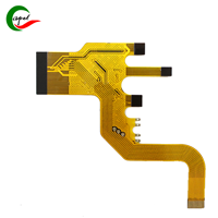 Automotive Double-Sided Flexible PCB
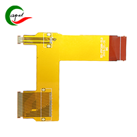 Medical Device Double-Sided Flexible PCB
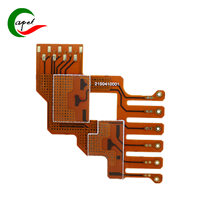 Medical Device Double-Sided Flexible PCB
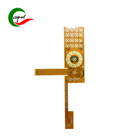 Medical Device Double-Sided Flexible PCB
 Medical Device Double-Sided Flexible PCB
 Double-sided Flexible PCB for Display


 Wechat
 +86 13670210335
 +86 13670210335
 E-mail