

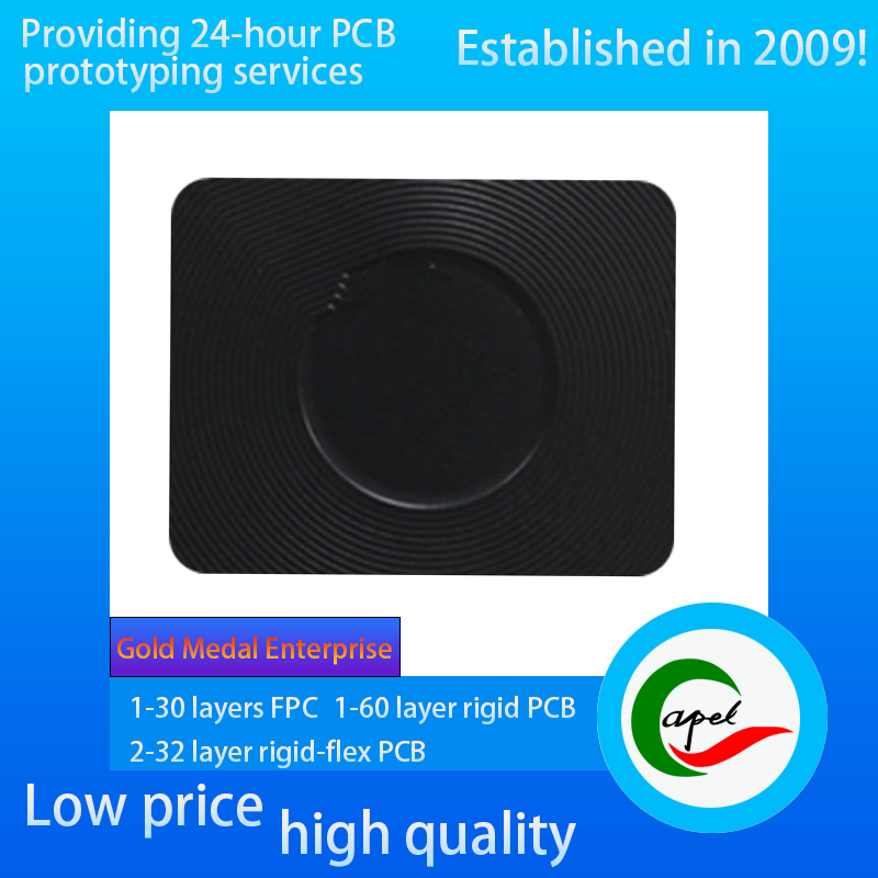
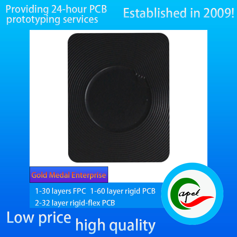
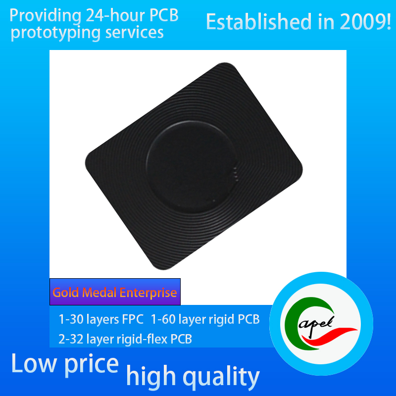
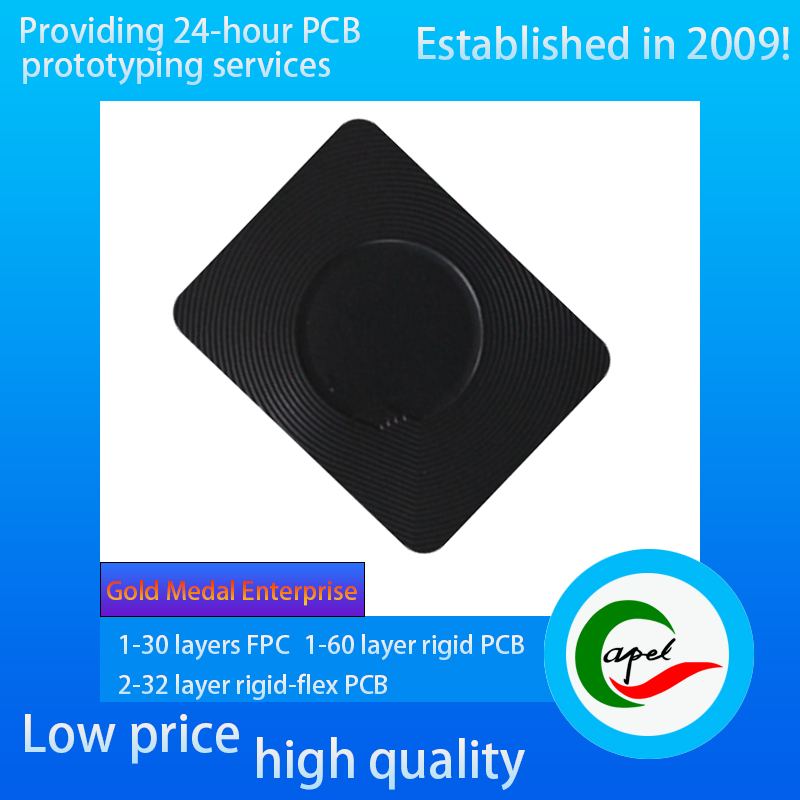

Cell phone wireless charging FPC
A short introduction:
Type: Mobile phone wireless charging FPC
Minimum line width/line spacing: 0.06mm/0.08mm
Number of layers: 2
Thickness: 0.15mm
Surface treatment: Immersion gold
Kaboer's services:
Support customized 1-30 layers FPC flexible PCB, 2-32 layers rigid-flex PCB, 1-60 layers rigid PCB, reliable fast turnaround PCB prototyping Rapid SMT PCB Assembly
Industries We Serve:
Medical devices, IoT, TUT, UAVs, Aviation, Automotive, Telecom, Consumer Electronics, Military, Aerospace, Industrial Controls, Artificial Intelligence, Electric Vehicles, etc. ......
If you have related needs, please feel free to send us an email by clicking the button below.
Type: Flexible Printed Circuit (FPC) for wireless charging of cell phones, designed for wireless charging protocols such as the Qi standard, with excellent high-frequency signal transmission performance and spatial adaptability. Whether it is built-in wireless charging module (such as the back of the body coil connected to the motherboard), ultra-thin wireless charging base (thickness ≤ 5mm), or car cell phone wireless charging (curved surface fit design), can be flexibly adapted to the compact space layout, to realize the efficient transmission of electromagnetic induction signals (100-205kHz band) and control signals, instead of the traditional rigid wiring, to enhance the integration of the charging module and heat dissipation efficiency. 2. Precise parameters and performance guarantee.
Minimum wire width/spacing: 0.06mm/0.08mm for high precision. This parameter is optimized for the characteristics of wireless charging high-frequency signals: 0.06mm line width ensures lower loss of high-frequency inductive signal transmission (attenuation rate ≤ 0.3dB/m), reducing energy waste; 0.08mm line spacing realizes dense wiring in the limited space of the wiring to support parallel transmission of coil driving signals, temperature detection signals, and overcurrent protection signals, and to avoid interruption of charging caused by crosstalk signals (anti-interference capability ≥ 60dB). The anti-interference capability is ≥60dB, which ensures the charging process is stable and continuous.
Layers: 2-layer structure design, precise isolation of functions through scientific layering:
Signal layer: adopts impedance matching design (target impedance 50Ω±10%), optimizes the transmission path of high-frequency inductive signals, reduces signal reflection, and ensures that the charging energy conversion rate is ≥85% (under Qi standard);
Ground layer: a large-area copper foil covers to form an EMI shielding barrier, which not only reduces the interference of the magnetic field of the coil on other circuits of the cell phone (EMI suppression ≥ 55dB), but also reduces the interference of the coil on other circuits of the cell phone. Ground layer: A large area of copper foil covers the electromagnetic shielding barrier, which not only reduces the interference of the magnetic field of the coil on other circuits of the cell phone (EMI suppression ≥55dB), but also reduces the influence of the external electromagnetic environment (e.g., Wi-Fi signals) on the charging, which is especially suitable for the complex electromagnetic environment inside the cell phone.
The synergy of the two layers enhances the charging efficiency and strengthens the safety protection response speed (overcurrent protection trigger time ≤ 10ms).
Thickness: 0.15mm thin and light, perfectly suited to the “ultra-thin” design needs of cell phones and wireless charging devices. In the built-in cell phone scenario (body thickness ≤ 8mm), it can significantly reduce the extrusion of the row of wires on the battery capacity (releasing ≥ 5% of the internal space); in the wireless charging base, it supports the close fit of the coil and the motherboard (spacing ≤ 2mm), reducing the loss of energy transmission, while enhancing the efficiency of the equipment heat dissipation (the temperature is lowered by 3-5 ℃).
Surface treatment: the use of immersed gold technology (nickel layer thickness ≥ 5μm, gold layer thickness ≥ 0.05μm), bringing multiple consumer-grade advantages:
excellent conductivity of the gold layer, the contact resistance ≤ 8mΩ, reduce high-frequency signal transmission loss, help charge power increase (support 15W/20W fast charging);
immersed gold plating layer corrosion resistance, can withstand the cell phone internal oil, sweat erosion (through the 48-hour salt spray test without rust), to avoid long-term use The immersed gold plating is highly corrosion-resistant and can withstand the erosion of oil, dirt and sweat inside the mobile phone (no rusting after 48 hours of salt spray test), avoiding the “intermittent charging and decreased efficiency” caused by the oxidization of the contacts after long-term use;
enhances the reliability of the soldering joints and ensures that the welded parts of the wires and coil terminals and the main control chip do not fall off in the high-temperature charging environment (≤60 ℃) to prolong the service life of the equipment (design life ≥ 10,000 charging cycles).
Kaboer Flexible PCB & Rigid-Flex PCB Process Capability
| Category | Process Capability | Category | Process Capability |
| Production Type |
Single layer FPC / Double layers FPC Multi-layer FPC / Aluminum PCBs Rigid-Flex PCB |
Layers Number |
1-30 layers FPC 2-32 layers Rigid-FlexPCB 1-60 layers Rigid PCB HDI Boards |
| Max Manufacture Size |
Single layer FPC 4000mm Double layers FPC 1200mm Multi-layers FPC 750mm Rigid-Flex PCB 750mm |
Insulating Layer Thickness |
27.5um /37.5/ 50um /65/ 75um / 100um / 125um / 150um |
| Board Thickness |
FPC 0.06mm - 0.4mm Rigid-Flex PCB 0.25 - 6.0mm |
Tolerance of PTH Size |
±0.075mm |
| Surface Finish |
Immersion Gold/Immersion Silver/Gold Plating/Tin Plating/OSP |
Stiffener | FR4 / PI / PET / SUS / PSA/Alu |
| Semicircle Orifice Size | Min 0.4mm | Min Line Space/ width | 0.045mm/0.045mm |
| Thickness Tolerance | ±0.03mm | Impedance | 50Ω-120Ω |
| Copper Foil Thickness | 9um/12um / 18um / 35um / 70um/100um |
Impedance Controlled Tolerance |
±10% |
|
Tolerance of NPTH Size |
±0.05mm | The Min Flush Width | 0.80mm |
| Min Via Hole | 0.1mm |
Implement Standard |
GB / IPC-650 / IPC-6012 / IPC-6013II / IPC-6013III |


![]()
Kaboer manufacturing PCBs since 2009. Professional technology and high-precision Printed Circuit Boards involved in Medical, IOT, UAV, Aviation, Automotive, Aerospace, Industrial Control, Artificial Intelligence, Consumer Electronics etc..


 English
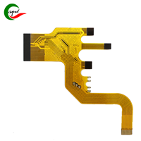 Automotive Double-Sided Flexible PCB
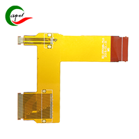 Medical Device Double-Sided Flexible PCB
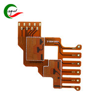 Medical Device Double-Sided Flexible PCB
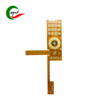 Medical Device Double-Sided Flexible PCB
 Medical Device Double-Sided Flexible PCB
 Double-sided Flexible PCB for Display


 Wechat
 +86 13670210335
 +86 13670210335
 E-mail