
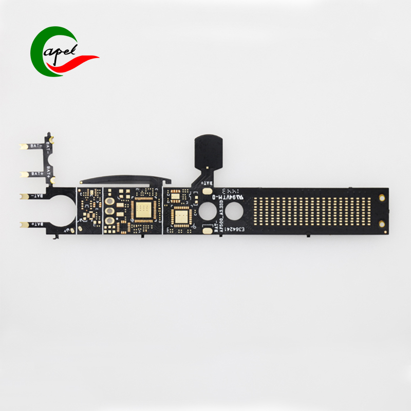

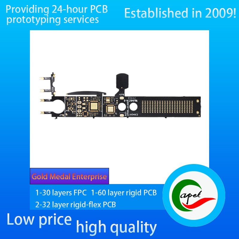
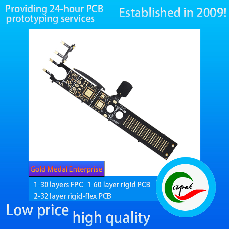
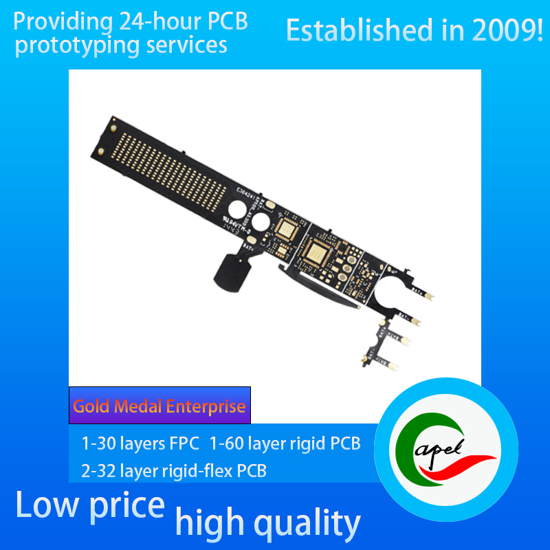

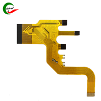
Static Bracelet FPC
A short introduction:
Type: Static Bracelet FPC
Minimum Line Width/Line Spacing: 0.1mm/0.1mm
Number of Layers: 2 Layers
Thickness: 0.12mm
Surface Finish: Immersion Gold 1 micro inch
Kaboer's Services:
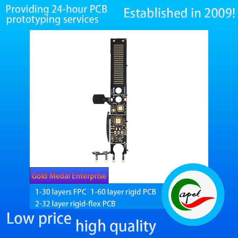
Support Customized 1-30 Layer FPC Flexible PCB, 2-32 Layers Rigid-Flexible Circuit Boards, 1-60 Layers Rigid PCB, Reliable Fast Turnaround PCB Prototyping Rapid SMT PCB Assembly
Industries We Serve:
Medical devices, IoT, TUT, UAVs, Aviation, Automotive, Telecom, Consumer Electronics, Military, Aerospace, Industrial Controls, Artificial Intelligence, Electric Vehicles, etc. ......
If you have related needs, please feel free to send us an email by clicking the button below.
Type: Flexible Circuit Board (FPC) for electrostatic bracelet, specially designed for human body electrostatic discharge, with low impedance conductivity and flexible wearable characteristics. Whether it is a wired electrostatic bracelet (connected to the grounding wire), wireless electrostatic bracelet (through Bluetooth to monitor the grounding status), or wristband type, finger sleeve type anti-static equipment, can be flexibly adapted to the curved structure of the bracelet (fit the curvature of the wrist) and the lightweight design (the overall weight of ≤ 5g), to achieve the human body static electricity through the FPC link to the earth quickly, instead of the traditional metal conductor, to achieve a balance between the effect of protection and wearing comfort. 2. Fine parameters and performance guarantee
Minimum line width/spacing: 0.1mm/0.1mm symmetrical high-precision standard. This parameter is specially optimized for electrostatic transmission characteristics: 0.1mm line width ensures that the conductive link impedance ≤ 100MΩ (in accordance with ANSI/ESD S20.20 standard), to meet the demand for rapid release of electrostatic discharge (release time ≤ 1 second); 0.1mm symmetrical spacing to achieve a multi-stranded conductive path in parallel design within a limited space (a single FPC to support the conductive path of 3-5 independent), even if the single Even if a single line is slightly worn out, the redundant paths can still protect the continuity of conductivity and avoid the risk of “protection interruption” (line redundancy design reduces the failure rate by 60%).
Layers: 2-layer structure design, through the scientific layering to achieve “conductive + safety” double protection:
Conductive layer: the use of high-purity copper foil (purity ≥ 99.9%) as the main electrical path, covered with gold-immersed layer to enhance the conductivity, to ensure that the human body static electricity (usually 1,000-15,000V) through the layer of rapid conduction to avoid the accumulation of charge safety isolation layer: local coverage of insulating substrate to form a safety barrier, the contact area between the conductive layer and human skin is controlled in a reasonable range (≤10mm²), which not only ensures reliable contact between the electrodes and the skin, but also avoids skin irritation caused by large-area metal contact (especially suitable for long-term wearing scenarios of more than 8 hours).
The two layers work in tandem to ensure low impedance conductivity while balancing “protection efficiency” and “wearability” through structural design.
Thickness: The ultra-thin feature of only 0.12mm is perfectly suited to the “lightweight and skin-feeling” design requirements of electrostatic bracelets. In the wristband type bracelet, it can significantly reduce the impact of FPC on the softness of the strap (the bending angle of the strap ≥120° without stiffness) and ensure that it fits the wrist curve when wearing (suitable for people with wrist circumference of 15-22cm); in the finger cuff type bracelet, it can be flexibly deformed with the finger activities (minimum bending radius R=0.3mm) without affecting the fine operations (such as chip soldering, circuit board assembly).
Surface treatment: the use of immersed gold 1 micro-inch process (nickel layer thickness ≥ 3μm, gold layer thickness ≥ 0.025μm), bringing multiple protection level advantages:
excellent conductivity of the gold layer, contact resistance ≤ 50mΩ, to ensure that the electrostatic discharge path impedance is stable (long-term use of impedance rate of change of ≤ 5%), to avoid oxidation due to the "conductive failure ";
sunken gold plating layer is resistant to sweat corrosion (no rust corrosion through 1000 hours of artificial sweat immersion test), adapting to the erosion of skin secretions when operators wear it for a long time, prolonging the service life of the bracelet (design life ≥ 1 year);
gold layer biocompatibility in line with the ISO 10993 standard, no risk of nickel release (release of nickel ions ≤ 0.5μg/cm²/ The gold layer is biocompatible with ISO 10993 standard, without the risk of nickel release (nickel ion release ≤0.5μg/cm²/week), avoiding skin irritation when worn by allergic personnel.
Kaboer Flexible PCB & Rigid-Flex PCB Process Capability
| Category | Process Capability | Category | Process Capability |
| Production Type |
Single layer FPC / Double layers FPC Multi-layer FPC / Aluminum PCBs Rigid-Flex PCB |
Layers Number |
1-30 layers FPC 2-32 layers Rigid-FlexPCB 1-60 layers Rigid PCB HDI Boards |
| Max Manufacture Size |
Single layer FPC 4000mm Double layers FPC 1200mm Multi-layers FPC 750mm Rigid-Flex PCB 750mm |
Insulating Layer Thickness |
27.5um /37.5/ 50um /65/ 75um / 100um / 125um / 150um |
| Board Thickness |
FPC 0.06mm - 0.4mm Rigid-Flex PCB 0.25 - 6.0mm |
Tolerance of PTH Size |
±0.075mm |
| Surface Finish |
Immersion Gold/Immersion Silver/Gold Plating/Tin Plating/OSP |
Stiffener | FR4 / PI / PET / SUS / PSA/Alu |
| Semicircle Orifice Size | Min 0.4mm | Min Line Space/ width | 0.045mm/0.045mm |
| Thickness Tolerance | ±0.03mm | Impedance | 50Ω-120Ω |
| Copper Foil Thickness | 9um/12um / 18um / 35um / 70um/100um |
Impedance Controlled Tolerance |
±10% |
|
Tolerance of NPTH Size |
±0.05mm | The Min Flush Width | 0.80mm |
| Min Via Hole | 0.1mm |
Implement Standard |
GB / IPC-650 / IPC-6012 / IPC-6013II / IPC-6013III |


![]()
Kaboer manufacturing PCBs since 2009. Professional technology and high-precision Printed Circuit Boards involved in Medical, IOT, UAV, Aviation, Automotive, Aerospace, Industrial Control, Artificial Intelligence, Consumer Electronics etc..


 English
 Automotive Double-Sided Flexible PCB
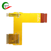 Medical Device Double-Sided Flexible PCB
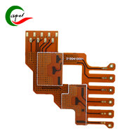 Medical Device Double-Sided Flexible PCB
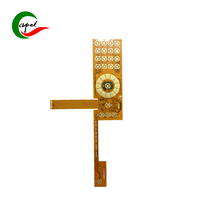 Medical Device Double-Sided Flexible PCB
 Medical Device Double-Sided Flexible PCB
 Double-sided Flexible PCB for Display


 Wechat
 +86 13670210335
 +86 13670210335
 E-mail