
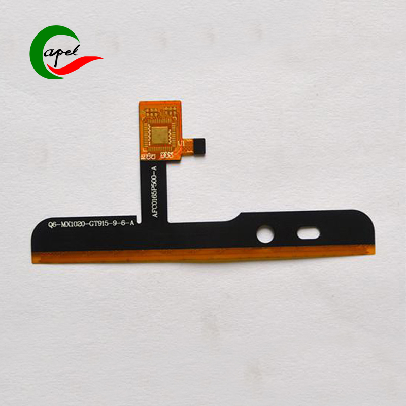


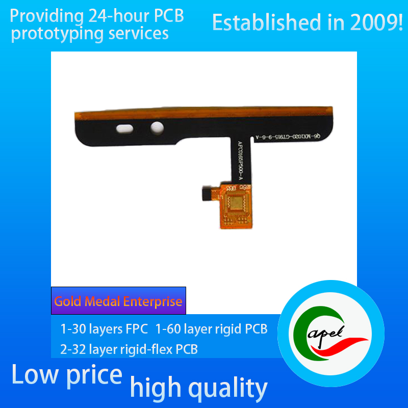
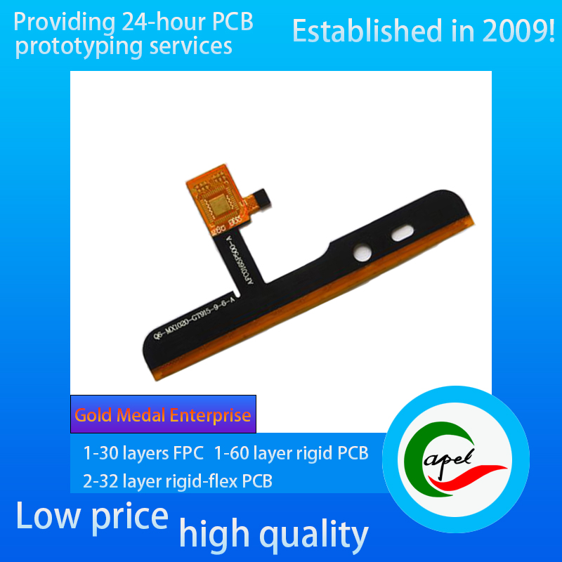
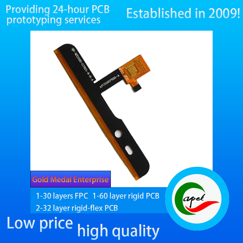

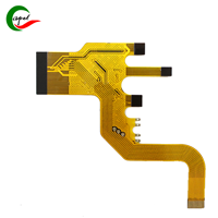
Tablet Module FPC
A short introduction:
Type: Tablet Module FPC
Minimum Line Width/Line Spacing: 0.07mm/0.06mm
Number of Layers: 2 Layers
Thickness: 0.3mm
Surface Finish: Immersion Gold 2 micro inches
Kaboer's Services:
Support Customized 1-30 Layer FPC Flexible PCB, 2-32 Layer Rigid-Flexible Circuit Boards, 1-60 Layer Rigid PCB, Reliable Fast Turnaround PCB prototyping, rapid SMT PCB assembly
Industries We Serve:
Medical devices, IoT, TUT, drones, aerospace, automotive, telecom, consumer electronics, military, aerospace, industrial control, AI, electric vehicles, etc. ......
If you have related needs, please feel free to send us an email by clicking the button below.
Type: Tablet PC module-specific flexible circuit board (FPC), designed for tablet internal multi-module synergistic design, adapted to the screen driver module, front / rear camera module, capacitive touch module, battery management module and other core scenarios. Whether it is a 10.9-inch thin and light tablet (body thickness ≤ 6.5mm), a 2.5K resolution educational tablet, or a professional creative tablet with stylus support, it can be flexibly adapted to the compact internal layout (e.g., millimeter gap between the screen and the motherboard, and the bending axis of the foldable screen), and realizes the parallel transmission of high-bandwidth signals (e.g., MIPI-DSI display protocol, USB 3.2 data transmission) and control commands, replacing the traditional rigid rows. Parallel transmission of high-bandwidth signals (e.g. MIPI-DSI display protocol, USB 3.2 data transmission) and control commands, replacing the traditional rigid wiring to improve device integration and space utilization.
Minimum line width/spacing: 0.07mm/0.06mm for high precision. This parameter is optimized for the high-frequency signal characteristics of the flat panel multi-module: 0.07mm line width to ensure that the 2K/4K display signals (transmission rate ≥ 8Gbps) lower transmission loss (signal attenuation rate of ≤ 0.15dB / m), reducing the loss of picture quality details; 0.06mm line spacing in the limited space of the wiring to achieve high-density cabling (a single row of lines to support ≥ 30 independent signals), to support the screen drive signals, touch coordinate signals, camera coordinates, signals, and so on. Parallel transmission of screen drive signals, touch coordinate signals, camera data signals, to avoid signal crosstalk caused by “screen flicker, touch drift” (crosstalk rejection ratio ≥ 75dB), to ensure frame synchronization during 4K video playback (frame delay ≤ 10ms).
Layers: 2-layer structure design to achieve precise isolation of functions through scientific layering and solve the problem of multi-module signal interference:
Signal Layer: Differential routing and equal-length wiring design to optimize the transmission path of MIPI display signals and USB data signals, to match the bandwidth requirements of high-resolution screens (e.g., 2560×1600 pixels) to ensure that the edges of the screen are free from blurring;
Power/Grounding Layer: Integration of power supply lines and large-area grounding copper foil to ensure frame synchronization during 4K video playback (frame delay ≤ 10ms). Power/Ground Layer: Integrated power supply lines and large grounding copper foil provide stable power supply (power ripple ≤15mV) for the screen backlight and camera sensors, and form an electromagnetic shielding barrier (EMI suppression ≥60dB) to isolate the interference of the motherboard's RF module (e.g., Wi-Fi 6) with the display signals, which is especially suitable for strong electromagnetic environments of full-metal-body flat panels.
The two-layer synergy ensures high-speed signal transmission while simplifying the circuit structure, which is suitable for the “lightweight” design requirements of flat panels.
Thickness: The optimized thickness of 0.3mm perfectly balances “structural stability” and “spatial adaptability”. In the flat panel screen module, it can support the rigid connection between the screen and the motherboard (tensile strength ≥ 40N/cm), avoiding the breakage of the row of wires when opening and closing the protective sleeve; in the folding axis of the foldable flat panel, it can maintain moderate flexibility (supporting the smallest bending radius R = 2mm), adapting to more than 100,000 times of folding operations (such as folding screen unfolding/closing), and at the same time, reducing signal attenuation caused by fatigue of the bending.
Surface treatment: the use of immersion gold 2 micro-inch process (nickel layer thickness ≥ 5μm, the thickness of the gold layer ≥ 0.05μm), to bring multiple consumer-grade advantages:
excellent conductivity of the gold layer, the contact resistance of ≤ 8mΩ, to reduce high-frequency signal transmission loss, to ensure the color reproduction of the 2K/4K screen (Delta E ≤ 2);
2 micro-inch thickened layer of corrosion-resistant gold can withstand the flat panel of internal perspiration, dust erosion (The 2 micro-inch thickened gold layer is highly corrosion-resistant, which can withstand sweat and dust erosion inside the flat panel (no corrosion after 72 hours of neutral salt spray test), and adapt to the skin contact scenarios when users are holding it;
enhances the reliability of the soldering joints and ensures that the soldering parts of the wires and the screen interface and camera connector do not loosen during long-term vibration (such as bumps when carrying), thus prolonging the service life of the device (design life ≥ 3 years).
Kaboer Flexible PCB & Rigid-Flex PCB Process Capability
| Category | Process Capability | Category | Process Capability |
| Production Type |
Single layer FPC / Double layers FPC Multi-layer FPC / Aluminum PCBs Rigid-Flex PCB |
Layers Number |
1-30 layers FPC 2-32 layers Rigid-FlexPCB 1-60 layers Rigid PCB HDI Boards |
| Max Manufacture Size |
Single layer FPC 4000mm Double layers FPC 1200mm Multi-layers FPC 750mm Rigid-Flex PCB 750mm |
Insulating Layer Thickness |
27.5um /37.5/ 50um /65/ 75um / 100um / 125um / 150um |
| Board Thickness |
FPC 0.06mm - 0.4mm Rigid-Flex PCB 0.25 - 6.0mm |
Tolerance of PTH Size |
±0.075mm |
| Surface Finish |
Immersion Gold/Immersion Silver/Gold Plating/Tin Plating/OSP |
Stiffener | FR4 / PI / PET / SUS / PSA/Alu |
| Semicircle Orifice Size | Min 0.4mm | Min Line Space/ width | 0.045mm/0.045mm |
| Thickness Tolerance | ±0.03mm | Impedance | 50Ω-120Ω |
| Copper Foil Thickness | 9um/12um / 18um / 35um / 70um/100um |
Impedance Controlled Tolerance |
±10% |
|
Tolerance of NPTH Size |
±0.05mm | The Min Flush Width | 0.80mm |
| Min Via Hole | 0.1mm |
Implement Standard |
GB / IPC-650 / IPC-6012 / IPC-6013II / IPC-6013III |


![]()
Kaboer manufacturing PCBs since 2009. Professional technology and high-precision Printed Circuit Boards involved in Medical, IOT, UAV, Aviation, Automotive, Aerospace, Industrial Control, Artificial Intelligence, Consumer Electronics etc..


 English
 Automotive Double-Sided Flexible PCB
 Medical Device Double-Sided Flexible PCB
 Medical Device Double-Sided Flexible PCB
 Medical Device Double-Sided Flexible PCB
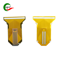 Medical Device Double-Sided Flexible PCB
 Double-sided Flexible PCB for Display


 Wechat
 +86 13670210335
 +86 13670210335
 E-mail