
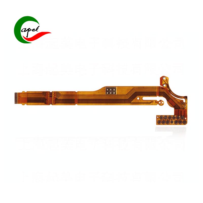

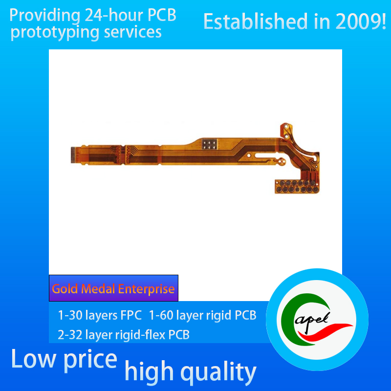
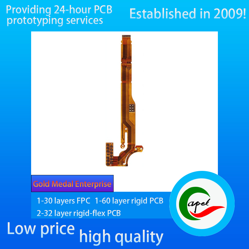
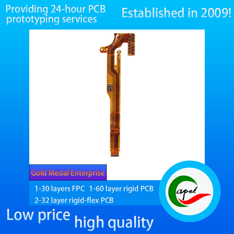
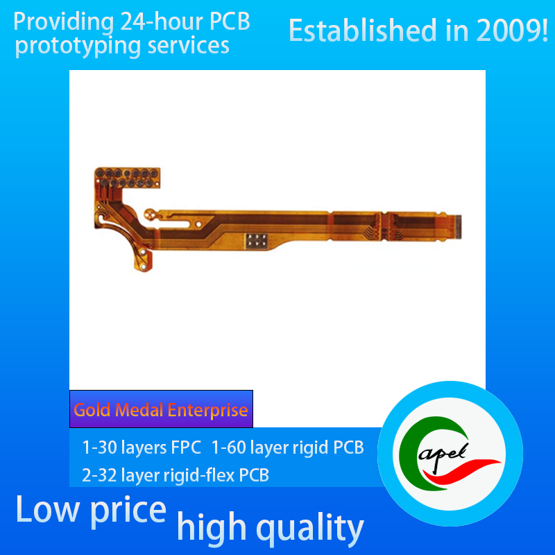

Tablet Antenna FPC
A short introduction:
Type: Tablet Antenna FPC
Minimum Line Width/Line Spacing: 0.08mm/0.075mm
Number of Layers: 2 Layers
Thickness: 0.2mm
Surface Finish: Immersion Gold 1 micro inch
Kaboer's Services:
Support Customized 1-30 Layer FPC Flexible PCB, 2-32 Layer Rigid-Flexible Circuit Boards, 1-60 Layer Rigid PCB, Reliable Fast Turnaround PCB prototyping, rapid SMT PCB assembly
Industries we serve:
Medical devices, IoT, TUT, drones, aerospace, automotive, telecom, consumer electronics, military, aerospace, industrial control, AI, electric vehicles, etc. ......
If you have related needs, please feel free to send us an email by clicking the button below.
Type: Tablet PC special antenna flexible circuit board (FPC), designed for wireless communication scenarios, adapted to Wi-Fi, 5G, Bluetooth, NFC and other multi-frequency band signal transceiver. Whether it is a 10.9-inch thin and light tablet (body thickness ≤ 6.8mm), folding screen tablet bezel area, or outdoor tablets supporting cellular networks, can be flexibly adapted to the curved bezel of the device, the back of the notch and other alien structures, instead of the traditional metal shrapnel antenna in a limited space (installation area of ≤ 10cm ²) to achieve full coverage of multi-frequency signals to meet the wireless needs of video conferencing, online games, outdoor navigation, and other scenes. It realizes full multi-band signal coverage in limited space (installation area ≤10cm²) and meets the wireless needs of video conference, online game, outdoor navigation, etc.
Minimum line width / line spacing: 0.08mm/0.075mm high precision standard. This parameter is optimized for the characteristics of high-frequency wireless signals: 0.08mm line width ensures lower 2.4GHz/5GHz signal transmission loss (attenuation rate ≤0.3dB@5GHz), which reduces signal attenuation when communicating through a wall or over long distances; 0.075mm line spacing realizes multiband antenna integration in a limited wiring space (a single FPC can integrate a Wi-Fi+Bluetooth dual band antenna), and isolates different bands through reasonable spacing. The FPC is designed to isolate different frequency band signals through reasonable spacing (band isolation degree ≥ 30dB), avoiding “network stuttering and disconnection” caused by mutual interference between 2.4GHz and 5GHz signals.
Layers: 2-layer structure design, through scientific layering to achieve “signal + ground” synergistic efficiency:
antenna radiation layer: copper foil etching to form a specific pattern (such as inverted F-shape, monopole structure), accurately matching the target band (2.4GHz band resonance frequency deviation of ≤ ± 5%), to ensure that the signal transmitting and receiving efficiency (gain of ≥ 2dBi @ 5GHz). ≥
Grounding reference layer: large area copper foil covers to form a “ground plane”, which not only serves as the reflective surface of the antenna to enhance the radiation efficiency (15% higher than the single-layer design), but also shields the flat panel from the internal screen and the electromagnetic interference of the battery (EMI suppression ≥ 55dB), which is especially suitable for strong electromagnetic environments of the flat panels with a full-metal body. Electromagnetic environment.
Two-layer synergy in reducing the size of the antenna at the same time, improve the stability of multi-band signal and anti-interference ability.
Thickness: 0.2mm ultra-thin, perfectly suited to the “zero waste of space” design requirements of flat panels. In the bezel area (width ≤ 8mm), it can closely fit the curved surface (curvature ≥ R5mm), without increasing the thickness of the device; when installed in the groove on the back, it can be slightly deformed with the equipment shell (tensile rate ≤ 5%), avoiding the antenna performance degradation due to the assembly stress, and at the same time, reserving more space for the battery and camera module.
Surface treatment: the use of immersed gold 1 micro-inch process (nickel layer thickness ≥ 3μm, gold layer thickness ≥ 0.025μm), to bring multiple high-frequency advantages:
excellent conductivity of the gold layer, reduce the antenna surface impedance (impedance deviation ≤ 5%), to ensure that the radiation efficiency of the high-frequency signals of the 5GHz (efficiency ≥ 60%), to enhance the stability of the peak rate of the Wi-Fi 6 of 1.2Gbps;
immersed gold plating layer of corrosion resistance, can withstand sweat inside the tablet Strong corrosion resistance of the immersed gold plating layer, which can resist the erosion of sweat and dust inside the flat panel (no rust and corrosion after 48 hours of neutral salt spray test), avoiding the “signal weakness and frequency band shift” caused by the oxidation of the copper foil after long-term use;
enhances the reliability of the soldering of the antenna and the RF module to ensure that the soldering points of the antenna and the RF interface of the motherboard are stable (contact resistance ≤ 10m m) in the contact of long-term vibration (e.g., bumps when carrying). Stable (contact resistance ≤ 10mΩ), prolonging the life of wireless function (design life ≥ 3 years).
Kaboer Flexible PCB & Rigid-Flex PCB Process Capability
| Category | Process Capability | Category | Process Capability |
| Production Type |
Single layer FPC / Double layers FPC Multi-layer FPC / Aluminum PCBs Rigid-Flex PCB |
Layers Number |
1-30 layers FPC 2-32 layers Rigid-FlexPCB 1-60 layers Rigid PCB HDI Boards |
| Max Manufacture Size |
Single layer FPC 4000mm Double layers FPC 1200mm Multi-layers FPC 750mm Rigid-Flex PCB 750mm |
Insulating Layer Thickness |
27.5um /37.5/ 50um /65/ 75um / 100um / 125um / 150um |
| Board Thickness |
FPC 0.06mm - 0.4mm Rigid-Flex PCB 0.25 - 6.0mm |
Tolerance of PTH Size |
±0.075mm |
| Surface Finish |
Immersion Gold/Immersion Silver/Gold Plating/Tin Plating/OSP |
Stiffener | FR4 / PI / PET / SUS / PSA/Alu |
| Semicircle Orifice Size | Min 0.4mm | Min Line Space/ width | 0.045mm/0.045mm |
| Thickness Tolerance | ±0.03mm | Impedance | 50Ω-120Ω |
| Copper Foil Thickness | 9um/12um / 18um / 35um / 70um/100um |
Impedance Controlled Tolerance |
±10% |
|
Tolerance of NPTH Size |
±0.05mm | The Min Flush Width | 0.80mm |
| Min Via Hole | 0.1mm |
Implement Standard |
GB / IPC-650 / IPC-6012 / IPC-6013II / IPC-6013III |


![]()
Kaboer manufacturing PCBs since 2009. Professional technology and high-precision Printed Circuit Boards involved in Medical, IOT, UAV, Aviation, Automotive, Aerospace, Industrial Control, Artificial Intelligence, Consumer Electronics etc..


 English
 Automotive Double-Sided Flexible PCB
 Medical Device Double-Sided Flexible PCB
 Medical Device Double-Sided Flexible PCB
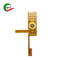 Medical Device Double-Sided Flexible PCB
 Medical Device Double-Sided Flexible PCB
 Double-sided Flexible PCB for Display


 Wechat
 +86 13670210335
 +86 13670210335
 E-mail