
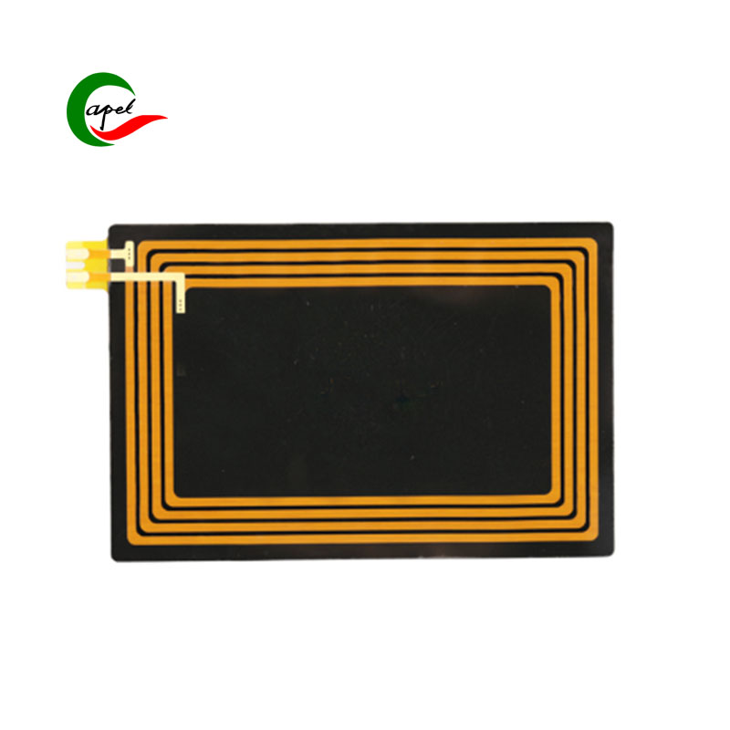

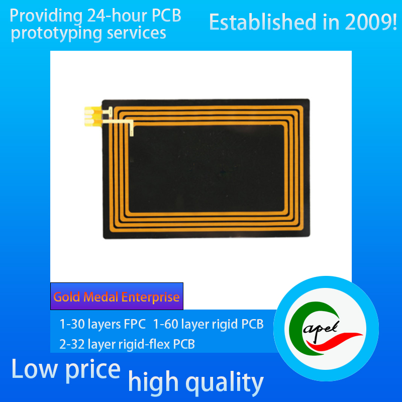
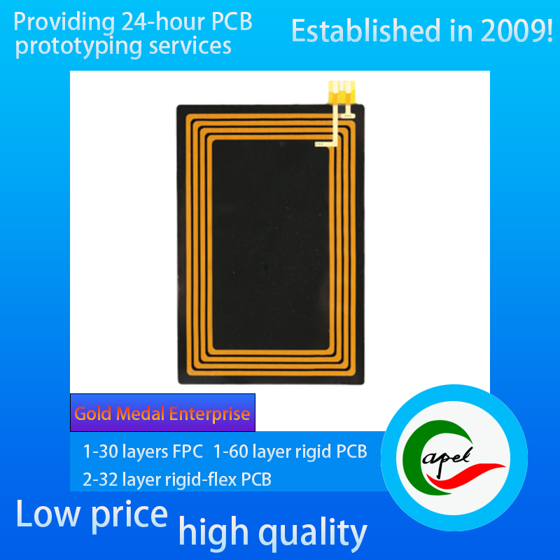
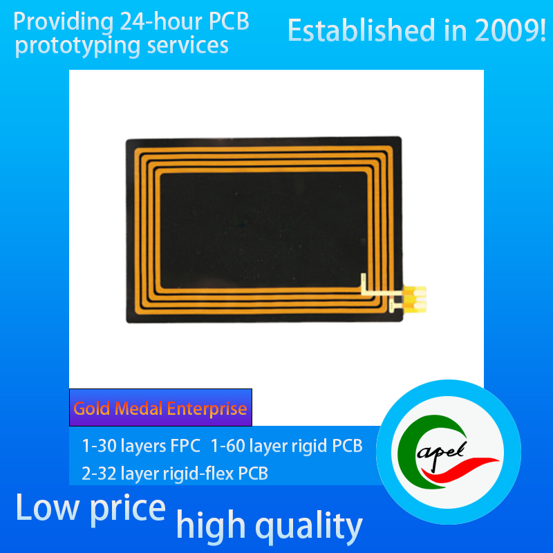
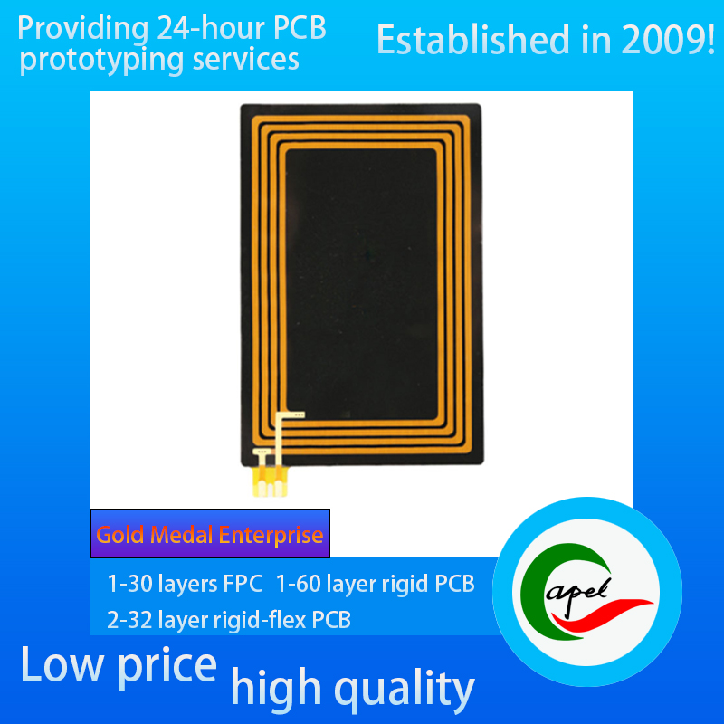

Cell Phone Antenna FPC
A short introduction:
Type: Cell Phone Antenna FPC
Minimum Line Width/Line Spacing: 1.02mm/0.48mm
Number of Layers: 1 Layer
Thickness: 0.08mm
Surface Finish: Immersion Gold
Kaboer's Services:
Support Customized 1-30 Layer FPC Flexible PCB, 2-32 Layers Rigid-Flexible Circuit Boards, 1-60 Layers Rigid PCB, Reliable Fast Turnaround PCB Prototyping. Rapid SMT PCB Assembly
Industries We Serve:
Medical Device, IoT, TUT, UAV, Aerospace, Automotive, Telecom, Consumer Electronics, Military, Aerospace, Industrial Controls, Artificial Intelligence, Electric Vehicles, etc. ......
If you have related needs, please feel free to send us an email by clicking the button below.
Type: Flexible Printed Circuit (FPC) for cell phone antennas, specially designed for smart phone wireless communication modules, with extreme flexibility and signal conduction performance. Whether it is the hidden antenna in the border of full-screen cell phone, the bent area antenna of folding screen cell phone, or the integrated antenna module supporting multiple frequency bands, it can be flexibly adapted to the complex spatial layout inside the cell phone (e.g., the middle frame of the body, the inside of the battery cover), and can realize the high efficiency of radiation and reception of signals in multiple frequency bands, such as 5G Sub-6GHz, millimeter wave, Wi-Fi 6E, Bluetooth 5.3, etc., and can replace the traditional metal shrapnel antenna. antenna, improving communication stability and device integration.
Minimum line width/spacing: 1.02mm/0.48mm optimized design, precisely adapted to the antenna signal radiation characteristics; 1.02mm line width ensures low-loss transmission of high-frequency signals (e.g., 5G 3.5GHz band) and reduces signal attenuation; 0.48mm spacing is reserved for the parallel wiring of multi-frequency antennas, which supports the independent transmission of 5G and Wi-Fi signals and avoids interband interference, ensuring the efficient radiation and reception of calls, Internet access, Bluetooth 5.3 and other multi-frequency antennas. It supports independent transmission of 5G and Wi-Fi signals, avoiding interference between frequency bands and guaranteeing signal stability during simultaneous operation of call, Internet access, Bluetooth connection, etc.
Layer: 1-layer structural design, realizing high efficiency of signal transmission through a minimalist structure. The single-layer layout reduces inter-layer signal reflection and loss, which is especially suitable for the radiation characteristics of high-frequency signals (signal radiation efficiency is increased by about 8%); at the same time, it simplifies the production process, ensures the consistency of the performance of each batch of products, and reduces the risk of signal fluctuations due to the tolerances of the multilayer structure, which is suitable for medium- and high-end cell phones with high requirements for communication stability.
Thickness: The extreme thinness of only 0.08mm, which perfectly fits the smartphone. Thin and light characteristics, perfectly suited to the “thin and light” design trend of smart phones (body thickness is generally <8mm). In the structure of cell phone's internal space, it can be installed close to the curved surface of the fuselage or slit, without occupying the layout space of core components (such as battery and camera), and at the same time, it improves the fit between the antenna and the fuselage, enhances the precision of the signal radiation direction, and reduces the dead space of the signal.
Surface treatment: Adopting the immersion gold process, it brings multiple performance advantages by depositing nickel-gold plating uniformly on the surface of the copper layer, which is a good choice for the surface treatment. Multiple performance advantages:
excellent conductivity of the gold layer, reducing high-frequency signal transmission loss (especially in the millimeter-wave band, signal attenuation is reduced by about 5%);
enhance the surface corrosion resistance, resisting the daily use of cell phones in the sweat, oil erosion, to avoid degradation of antenna performance due to oxidation;
enhance the reliability of the solder joints, to ensure that the antenna FPC is reliable. Enhance the reliability of the solder joints to ensure stable contact between the antenna FPC and the motherboard and RF module, reduce signal fluctuations caused by changes in contact resistance, and extend the communication life of the device.
| Category | Process Capability | Category | Process Capability |
| Production Type |
Single layer FPC / Double layers FPC Multi-layer FPC / Aluminum PCBs Rigid-Flex PCB |
Layers Number |
1-30 layers FPC 2-32 layers Rigid-FlexPCB 1-60 layers Rigid PCB HDI Boards |
| Max Manufacture Size |
Single layer FPC 4000mm Double layers FPC 1200mm Multi-layers FPC 750mm Rigid-Flex PCB 750mm |
Insulating Layer Thickness |
27.5um /37.5/ 50um /65/ 75um / 100um / 125um / 150um |
| Board Thickness |
FPC 0.06mm - 0.4mm Rigid-Flex PCB 0.25 - 6.0mm |
Tolerance of PTH Size |
±0.075mm |
| Surface Finish |
Immersion Gold/Immersion Silver/Gold Plating/Tin Plating/OSP |
Stiffener | FR4 / PI / PET / SUS / PSA/Alu |
| Semicircle Orifice Size | Min 0.4mm | Min Line Space/ width | 0.045mm/0.045mm |
| Thickness Tolerance | ±0.03mm | Impedance | 50Ω-120Ω |
| Copper Foil Thickness | 9um/12um / 18um / 35um / 70um/100um |
Impedance Controlled Tolerance |
±10% |
|
Tolerance of NPTH Size |
±0.05mm | The Min Flush Width | 0.80mm |
| Min Via Hole | 0.1mm |
Implement Standard |
GB / IPC-650 / IPC-6012 / IPC-6013II / IPC-6013III |


![]()
Kaboer manufacturing PCBs since 2009. Professional technology and high-precision Printed Circuit Boards involved in Medical, IOT, UAV, Aviation, Automotive, Aerospace, Industrial Control, Artificial Intelligence, Consumer Electronics etc..


 English
 Automotive Navigation Single-Sided Flexible PCB
 Automotive Navigation Single-Sided Flexible PCB
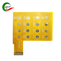 Single-Sided Flexible PCB for Automotive Applications
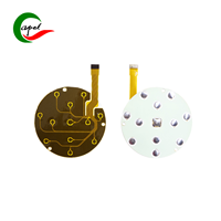 Medical Device Single-Sided Flexible PCB
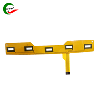
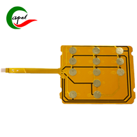 Single-Sided Keypad Flexible PCB
 Single-Sided Flexible PCB for Communication Equipment


 Wechat
 +86 13670210335
 +86 13670210335
 E-mail