
6 Layer HDI Flexible PCB For Industrial Control Sensors-Case
| Technical requirements | ||||||
| Product type | Multiple HDI Flexible Pcb Board | |||||
| Number of layer | 6 Layers | |||||
| Line width and line spacing | 0.05/0.05mm | |||||
| Board thickness | 0.2mm | |||||
| Copper Thickness | 12um | |||||
| Minimum Aperture | 0.1mm | |||||
| Flame Retardant | 94V0 | |||||
| Surface Treatment | Immersion Gold | |||||
| Solder Mask Color | Yellow | |||||
| Stiffness | Steel Sheet,FR4 | |||||
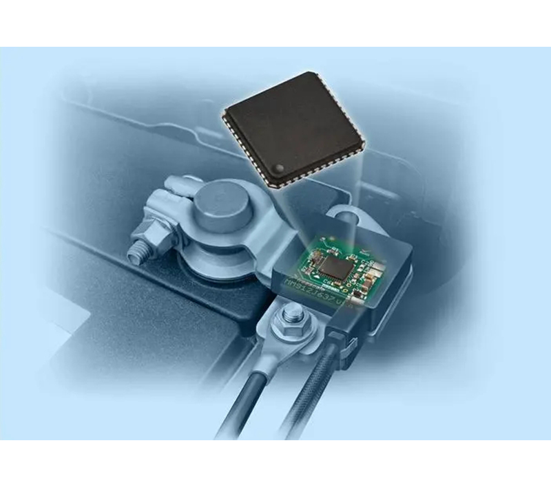
| Application | Industry Control | |||||
| Application Device | Sensor | |||||
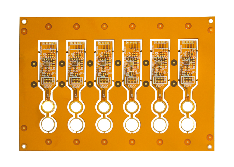
Case Analysis
Capel is a manufacturing company specializing in printed circuit boards (PCBs). They offer a range of services including PCB fabrication, PCB fabrication and assembly, HDI
PCB prototyping, quick turn rigid flex PCB, turnkey PCB assembly and flex circuit manufacturing. In this case, Capel focuses on the production of 6-layer HDI flexible PCBs
for industrial control applications, especially for use with sensor devices.
The technical innovation points of each product parameter are as follows:
Line width and line spacing:
The line width and line spacing of PCB are specified as 0.05/0.05mm. This represents a major innovation for the industry as it allows for the miniaturization of high-density circuits and electronic devices. It enables PCBs to accommodate more complex circuit designs and improves overall performance.
Board thickness:
Plate thickness is specified as 0.2mm. This low profile provides the flexibility required for flexible PCBs, making it suitable for applications that require PCBs to be bent or folded. The thinness also contributes to the overall lightweight design of the product. Copper thickness: Copper thickness is specified as 12um. This thin copper layer is an innovative feature that allows for better heat dissipation and lower resistance, improving signal integrity and performance.
Minimum aperture:
The minimum aperture is specified as 0.1mm. This small aperture size allows the creation of fine pitch designs and facilitates the mounting of micro components on PCBs. It enables higher packaging density and improved functionality.
Flame retardant:
PCB's flame retardant rating is 94V0, which is a high industry standard. This ensures the safety and reliability of the PCB, especially in applications where fire hazards may exist.
Surface Treatment:
The PCB is immersed in gold, providing a thin and even gold coating on the exposed copper surface. This surface finish provides excellent solderability, corrosion resistance, and ensures a flat solder mask surface.
Solder Mask Color:
Capel offers a yellow solder mask color option that not only provides a visually appealing finish but also improves contrast, providing better visibility during the assembly process or subsequent inspection.
Stiffness:
The PCB is designed with steel plate and FR4 material for a stiff combination. This allows for flexibility in the flexible PCB portions but rigidity in areas that require additional support. This innovative design ensures that the PCB can withstand bending and folding without affecting its functionality
In terms of solving technical problems for industry and equipment improvement, Capel consider the following points:
Enhanced Thermal Management:
As electronic devices continue to increase in complexity and miniaturization, improved thermal management is critical. Capel can focus on developing innovative solutions to effectively dissipate the heat generated by PCBs, such as using heat sinks or using advanced materials with better thermal conductivity.
Enhanced Signal Integrity:
As the demands of high-speed and high-frequency applications grow, there is a need for improved signal integrity. Capel can invest in research and development to minimize signal loss and noise, such as leveraging advanced signal integrity simulation tools and techniques.
Advanced flexible PCB manufacturing technology:
Flexible PCB has unique advantages in flexibility and compactness. Capel can explore advanced manufacturing technologies such as laser processing to produce complex and precise flexible PCB designs. This could lead to advances in miniaturization, increased circuit density, and improved reliability.
Advanced HDI manufacturing technology:
High-density interconnect (HDI) manufacturing technology enables the miniaturization of electronic devices while ensuring reliable performance. Capel can invest in advanced HDI manufacturing technologies such as laser drilling and sequential build-up to further improve PCB density, reliability and overall performance
Post time: Sep-09-2023
Back


