
Introduction: Technical Challenges in Automotive Electronics and Capel’s Innovations
As autonomous driving evolves toward L5 and electric vehicle (EV) battery management systems (BMS) demand higher energy density and safety, traditional PCB technologies struggle to address critical issues:
- Thermal Runaway Risks: ECU chipsets exceed 80W power consumption, with localized temperatures reaching 150°C
- 3D Integration Limits: BMS requires 256+ signal channels within 0.6mm board thickness
- Vibration Failures: Autonomous sensors must withstand 20G mechanical shocks
- Miniaturization Demands: LiDAR controllers require 0.03mm trace widths and 32-layer stacking
Capel Technology, leveraging 15 years of R&D, introduces a transformative solution combining high thermal conductivity PCBs (2.0W/mK), high-temperature resistant PCBs (-55°C~260°C), and 32-layer HDI buried/blind via technology (0.075mm microvias).
Section 1: Thermal Management Revolution for Autonomous Driving ECUs
1.1 ECU Thermal Challenges
- Nvidia Orin chipset heat flux density: 120W/cm²
- Conventional FR-4 substrates (0.3W/mK) cause 35% chip junction temperature overshoot
- 62% of ECU failures originate from thermal stress-induced solder fatigue
1.2 Capel’s Thermal Optimization Technology
Material Innovations:
- Nano-alumina reinforced polyimide substrates (2.0±0.2W/mK thermal conductivity)
- 3D copper pillar arrays (400% increased heat dissipation area)
Process Breakthroughs:
- Laser Direct Structuring (LDS) for optimized thermal pathways
- Hybrid stacking: 0.15mm ultra-thin copper + 2oz heavy copper layers
Performance Comparison:
| Parameter | Industry Standard | Capel Solution |
|---|---|---|
| Chip Junction Temp (°C) | 158 | 92 |
| Thermal Cycling Life | 1,500 cycles | 5,000+ cycles |
| Power Density (W/mm²) | 0.8 | 2.5 |
Section 2: BMS Wiring Revolution with 32-Layer HDI Technology
2.1 Industry Pain Points in BMS Design
- 800V platforms require 256+ cell voltage monitoring channels
- Conventional designs exceed space limits by 200% with 15% impedance mismatch
2.2 Capel’s High-Density Interconnect Solutions
Stackup Engineering:
- 1+N+1 any-layer HDI structure (32 layers at 0.035mm thickness)
- ±5% differential impedance control (10Gbps high-speed signals)
Microvia Technology:
- 0.075mm laser-blind vias (12:1 aspect ratio)
- <5% plating void rate (IPC-6012B Class 3 compliant)
Benchmark Results:
| Metric | Industry Average | Capel Solution |
|---|---|---|
| Channel Density (ch/cm²) | 48 | 126 |
| Voltage Accuracy (mV) | ±25 | ±5 |
| Signal Delay (ns/m) | 6.2 | 5.1 |
Section 3: Extreme Environment Reliability – MIL-SPEC Certified Solutions
3.1 High-Temperature Material Performance
- Glass Transition Temp (Tg): 280°C (IPC-TM-650 2.4.24C)
- Decomposition Temp (Td): 385°C (5% weight loss)
- Thermal Shock Survival: 1,000 cycles (-55°C↔260°C)
3.2 Proprietary Protection Technologies
- Plasma-grafted polymer coating (1,000h salt spray resistance)
- 3D EMI shielding cavities (60dB attenuation @10GHz)
Section 4: Case Study – Collaboration with Global Top 3 EV OEM
4.1 800V BMS Control Module
- Challenge: Integrate 512-channel AFE in 85×60mm space
- Solution:
- 20-layer rigid-flex PCB (3mm bend radius)
- Embedded temperature sensor network (0.03mm trace width)
- Localized metal-core cooling (0.15°C·cm²/W thermal resistance)
4.2 L4 Autonomous Domain Controller
- Results:
- 40% power reduction (72W → 43W)
- 66% size reduction vs. conventional designs
- ASIL-D functional safety certification
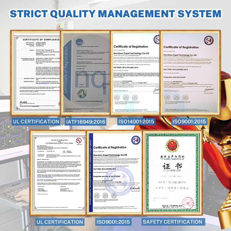
Section 5: Certifications and Quality Assurance
Capel’s quality system exceeds automotive standards:
- MIL-SPEC Certification: Compliant with GJB 9001C-2017
- Automotive Compliance: IATF 16949:2016 + AEC-Q200 validation
- Reliability Testing:
- 1,000h HAST (130°C/85% RH)
- 50G mechanical shock (MIL-STD-883H)
Conclusion: Next-Gen PCB Technology Roadmap
Capel is pioneering:
- Embedded passive components (30% space savings)
- Optoelectronic hybrid PCBs (0.2dB/cm loss @850nm)
- AI-driven DFM systems (15% yield improvement)
Contact our engineering team today to co-develop customized PCB solutions for your next-gen automotive electronics.
Post time: May-21-2025
Back


