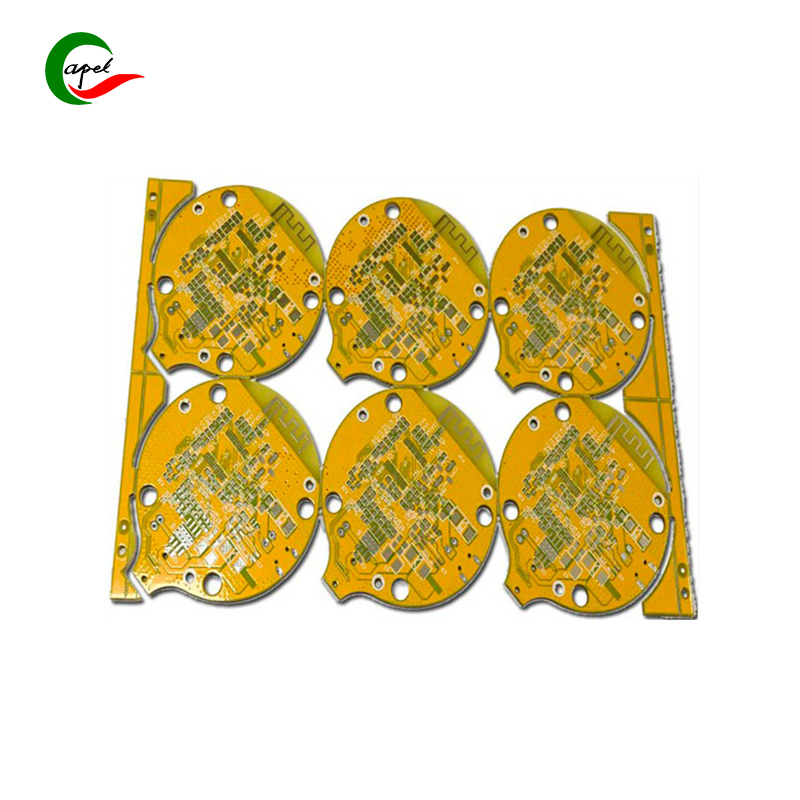
Double-Layer FR4 Printed Circuit Boards

PCB Process Capability
| No. | Project | Technical indicators |
| 1 | Layer | 1-60(layer) |
| 2 | Maximum processing area | 545 x 622 mm |
| 3 | Minimumboardthickness | 4(layer)0.40mm |
| 6(layer) 0.60mm | ||
| 8(layer) 0.8mm | ||
| 10(layer)1.0mm | ||
| 4 | Minimum line width | 0.0762mm |
| 5 | Minimum spacing | 0.0762mm |
| 6 | Minimum mechanical aperture | 0.15mm |
| 7 | Hole wall copper thickness | 0.015mm |
| 8 | Metallized aperture tolerance | ±0.05mm |
| 9 | Non-metallized aperture tolerance | ±0.025mm |
| 10 | Hole tolerance | ±0.05mm |
| 11 | Dimensional tolerance | ±0.076mm |
| 12 | Minimum solder bridge | 0.08mm |
| 13 | Insulation resistance | 1E+12Ω(normal) |
| 14 | Plate thickness ratio | 1:10 |
| 15 | Thermal shock | 288 ℃(4 times in 10 seconds) |
| 16 | Distorted and bent | ≤0.7% |
| 17 | Anti-electricity strength | >1.3KV/mm |
| 18 | Anti-stripping strength | 1.4N/mm |
| 19 | Solder resist hardness | ≥6H |
| 20 | Flame retardancy | 94V-0 |
| 21 | Impedance control | ±5% |
We do Printed Circuit Boards with 15 years' experience with our professionalism
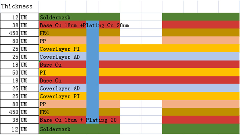
4 layer Flex-Rigid Boards
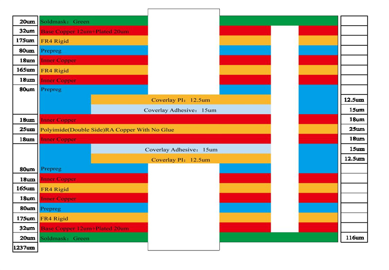
8 layer Rigid-Flex PCBs
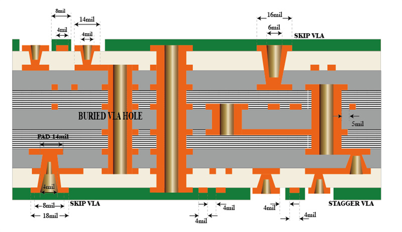
8 layer HDI Printed Circuit Boards
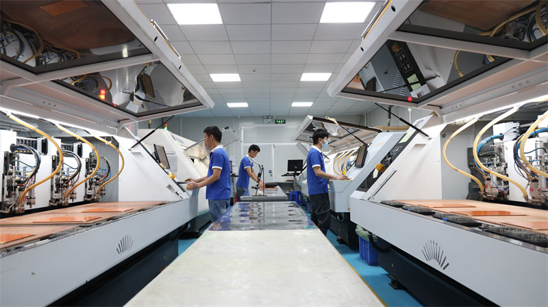
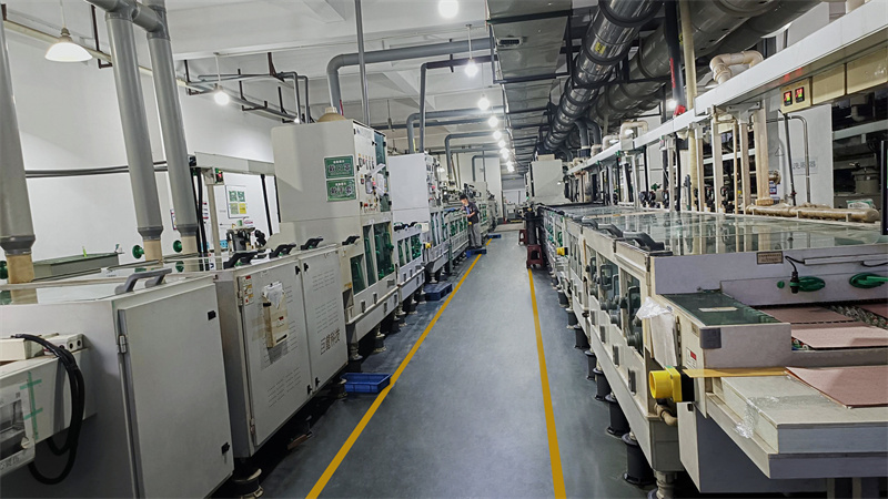
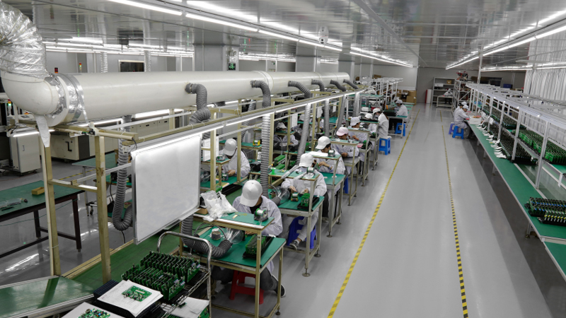
Testing and Inspection Equipment
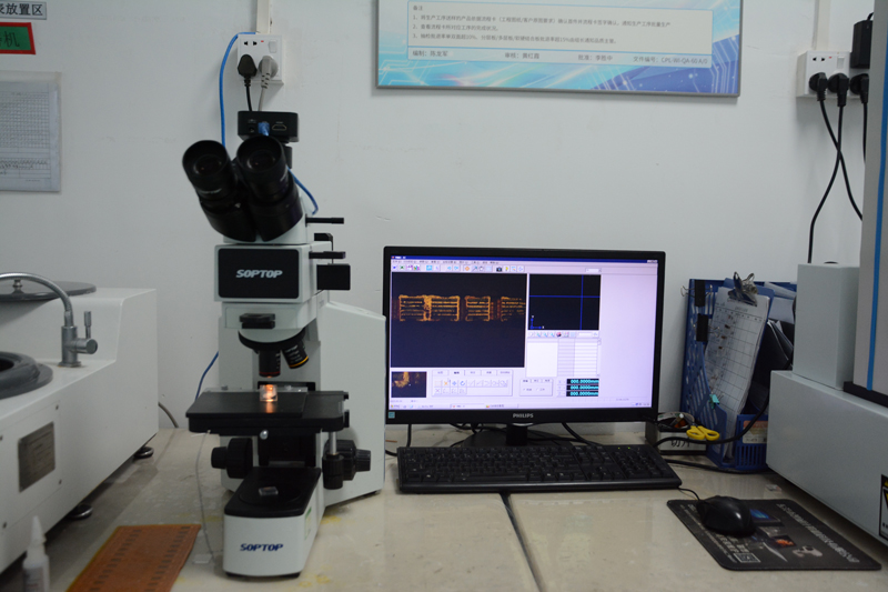
Microscope Testing
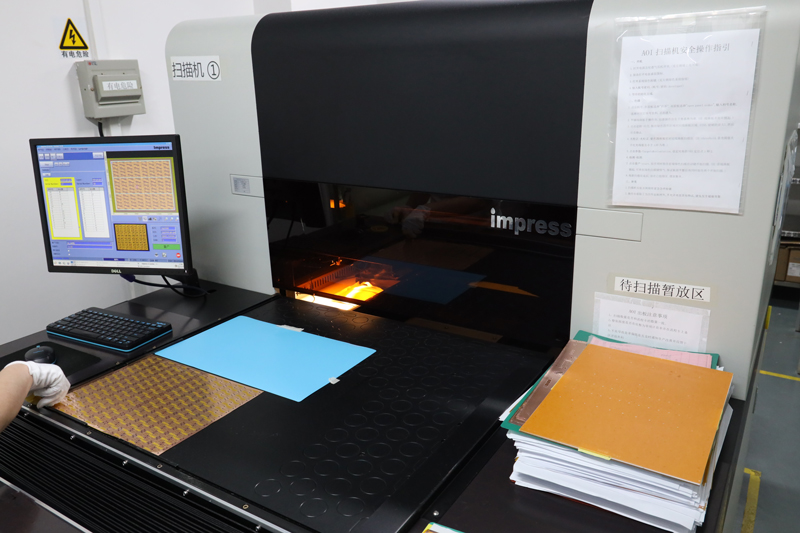
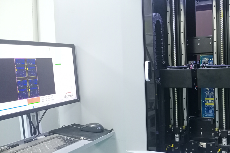
AOI Inspection
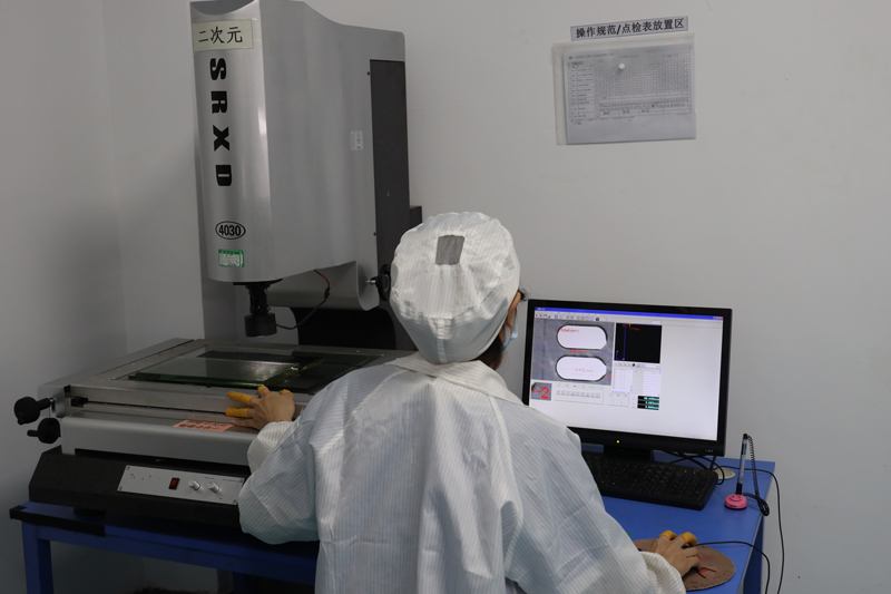
2D Testing
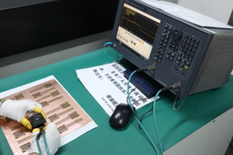
Impedance Testing
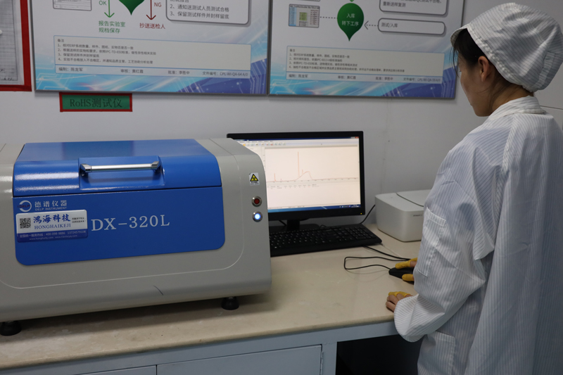
RoHS Testing
Flying Probe
Horizontal Tester
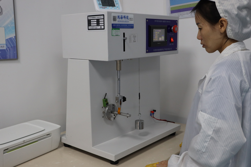
Bending Teste
Our Printed Circuit Boards Service
. Provide technical support Pre-sales and after-sales;
. Custom up to 40 layers, 1-2days Quick turn reliable prototyping, Component procurement, SMT Assembly;
. Caters to both Medical Device, Industrial Control, Automotive, Aviation, Consumer Electronics, IOT, UAV, Communications etc..
. Our teams of engineers and researchers are dedicated to fulfilling your requirements with precision and professionalism.

Double-layer FR4 Printed Circuit Boards applited in tablets
1. Power distribution: The power distribution of the tablet PC adopts double-layer FR4 PCB. These PCBs enable efficient routing of power lines to ensure proper voltage levels and distribution to the various components of the tablet, including the display, processor, memory and connectivity modules.
2. Signal routing: The double-layer FR4 PCB provides the necessary wiring and routing for signal transmission between different components and modules in the tablet computer. They connect various integrated circuits (ICs), connectors, sensors, and other components, ensuring proper communication and data transfer within devices.
3. Component Mounting: The double-layer FR4 PCB is designed to accommodate the mounting of various Surface Mount Technology (SMT) components in the tablet. These include microprocessors, memory modules, capacitors, resistors, integrated circuits and connectors. PCB layout and design ensures proper spacing and arrangement of components to optimize functionality and minimize signal interference.
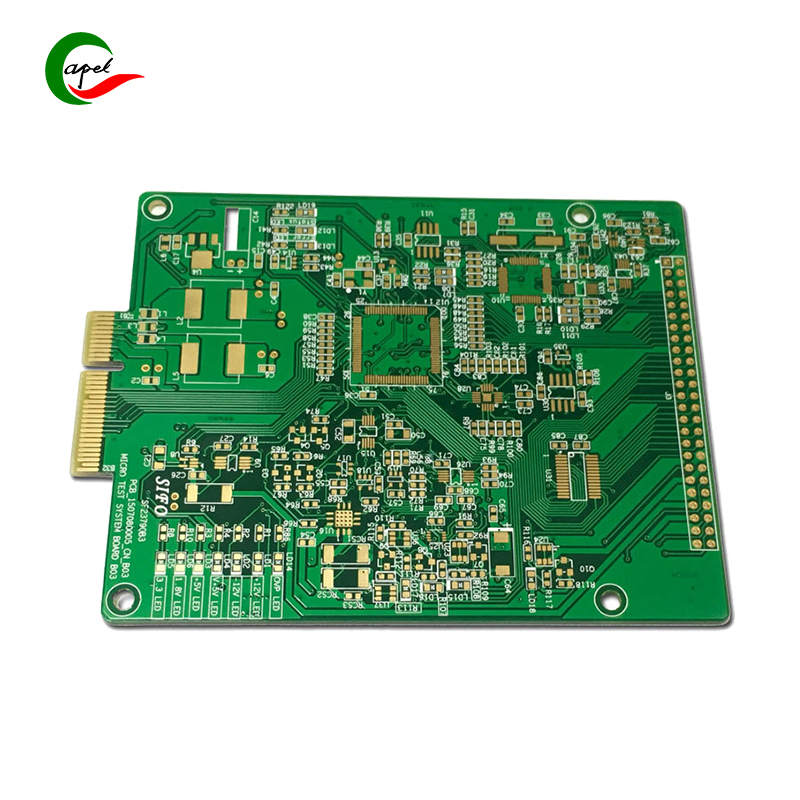
4. Size and compactness: FR4 PCBs are known for their durability and relatively thin profile, making them suitable for use in compact devices such as tablets. Double-layer FR4 PCBs allow for massive component densities in a limited space, enabling manufacturers to design thinner and lighter tablets without compromising functionality.
5. Cost-effectiveness: Compared with more advanced PCB substrates, FR4 is a relatively affordable material. Double-layer FR4 PCBs provide a cost-effective solution for tablet manufacturers who need to keep production costs low while maintaining quality and reliability.
How Double-layer FR4 Printed Circuit Boards enhance the performance and functionality of the tablets?
1. Ground and power planes: Two-layer FR4 PCBs typically have dedicated ground and power planes to help reduce noise and optimize power distribution. These planes act as a stable reference for signal integrity and minimize interference between different circuits and components.
2. Controlled impedance routing: In order to ensure reliable signal transmission and minimize signal attenuation, controlled impedance routing is used in the design of the double-layer FR4 PCB. These traces are carefully designed with a specific width and spacing to meet the impedance requirements of high-speed signals and interfaces such as USB, HDMI or WiFi.
3. EMI/EMC shielding: Double-layer FR4 PCB can use shielding technology to reduce electromagnetic interference (EMI) and ensure electromagnetic compatibility (EMC). Copper layers or shielding can be added to the PCB design to isolate sensitive circuitry from external EMI sources and prevent emissions that could interfere with other devices or systems.
4. High-frequency design considerations: For tablets containing high-frequency components or modules such as cellular connectivity (LTE/5G), GPS or Bluetooth, the design of a double-layer FR4 PCB needs to consider high-frequency performance. This includes impedance matching, controlled crosstalk and proper RF routing techniques to ensure optimum signal integrity and minimal transmission loss.